Common Emitter Amplifier
Amplifiers are circuits that allow a small signal to control a much larger one. Most amplifiers use transistors to accomplish this, but vacuum tubes are also common.
The common emitter amplifier is one of the most popular amplifier circuits. It uses a bipolar junction transistor in common emitter configuration.
In this article, we’ll cover the common emitter amplifier: how they work, and how to design circuits with them.
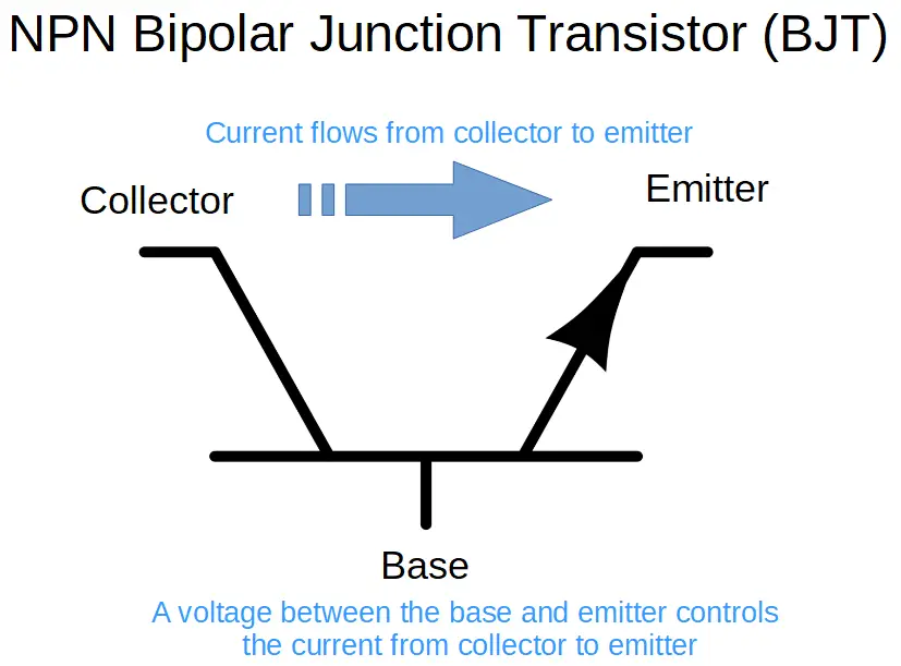
All transistors have three terminals. In bipolar junction transistors (BJTs), the three terminals are referred to as the base, emitter, and collector.
Since there are three terminals, there are naturally three possible orientations of a transistor within the circuit. Depending on the orientation, one of the three terminals must be ‘common’, or shared, between both the input and output. For this reason, the three configurations are called common emitter, common base, and common collector.
The common emitter configuration has a shared, or common, emitter. The input signal voltage is measured between the base and emitter, and the output signal voltage is measured between the collector and emitter.
The emitter is grounded, which is a quick way to check to see if the transistor is using the common emitter configuration.
This means that the emitter is at the electric potential (i.e. the lowest voltage point) against which both the input and output of the amplifier are measured.
How a Common Emitter Amplifier Works
In order to understand the common emitter amplifier, we have to think about the operation of bipolar junction transistors (BJTs).
Review of Bipolar Junction Transistors
The common emitter configuration uses a bipolar junction transistor (BJT) to amplify both voltage and current.
The primary function of the BJT is to allow a small voltage across or current through the base to control a much larger current between the collector and emitter.
NPN and PNP Transistors
There are two types of BJTs: NPN and PNP. These are the two possible ways of doping three alternating n-type and p-type doped regions in a semiconductor crystal.
A bipolar junction transistor is constructed by attaching a terminal to each of the three doped regions.
The main difference between the two types is that NPN transistors use electrons as the primary charge carriers, whereas PNP transistors use holes as the primary charge carriers. In each type of transistor, the charge carriers (either electrons or holes) move from the emitter, through the base, into the collector.
In PNP transistors the primary charge carriers are holes, which are positively charged. This means that current travels from the emitter through the collector.
In contrast, the primary charge carriers in NPN transistors are electrons, which are negatively charged. Electrons travel in the opposite direction as electric current, so the current flows from the collector to the emitter.
See the lesson on bipolar junction transistors (BJTs) for more information or a review.
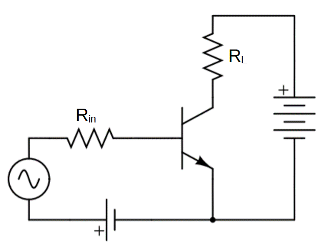
Common Emitter
In common emitter configuration, the primary input voltage is taken between the base and emitter, and the output voltage is measured between the collector and emitter.
There is also a voltage applied to the collector (called VCC or sometimes VC), and a corresponding current through the collector (called IC).
A Tale of Two Loops
The right side of the circuit diagram shows a loop between the collector, emitter, voltage source, and load resistance. A relatively high electric current flows around this loop in a counter-clockwise fashion.
The left side of the circuit also has a loop, with a much smaller current circulating clockwise through the base, emitter, and voltage source.
Thanks to the transistor’s ‘action‘, the loop on the left controls the loop on the right.
Since the left loop is connected to the base, any variation in the source voltage will result in a much larger (i.e. amplified) response in the right loop.
Thus the signal applied to the base will determine the output, which is taken between the load and collector.
The current through the emitter is the sum of the currents through the base and collector: IE = IB + IC
The load resistance is in series with the collector. The current gain (AI or β – beta) is the ratio between the current through the collector (IC) and the base (IB):
A_I=\beta=\frac{I_C}{I_B}The collector to emitter current ratio is also a useful quantity and is designated as α (alpha):
\alpha = \frac{I_C}{I_E}We can also solve for the collector current IC in terms of α and β:
I_C=\alpha I_E=\beta I_B
Voltage Divider Biased Amplifier
A more practical amplifier circuit is shown below. This configuration uses two resistors (R1 and R2) that form a voltage divider on the input (base).
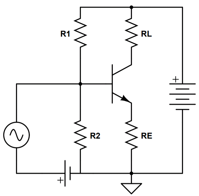
Using the voltage divider formula, we know that the voltage between the base and ground (VB) will be:
V_B=V_{CC}\frac{R_2}{R_1+R_2}This means that the base voltage is mediated by the voltage divider circuit, which helps to stabilize the transistor.
The current through the divider will depend on the total resistance of R1 + R2, using Ohm’s Law:
I=\frac{V_{CC}}{R_T}=\frac{V_{CC}}{R_1+R_2}Coupling Capacitors in Amplifiers
Many common amplifier circuits make use of coupling capacitors in order to filter out any DC components of an AC signal.
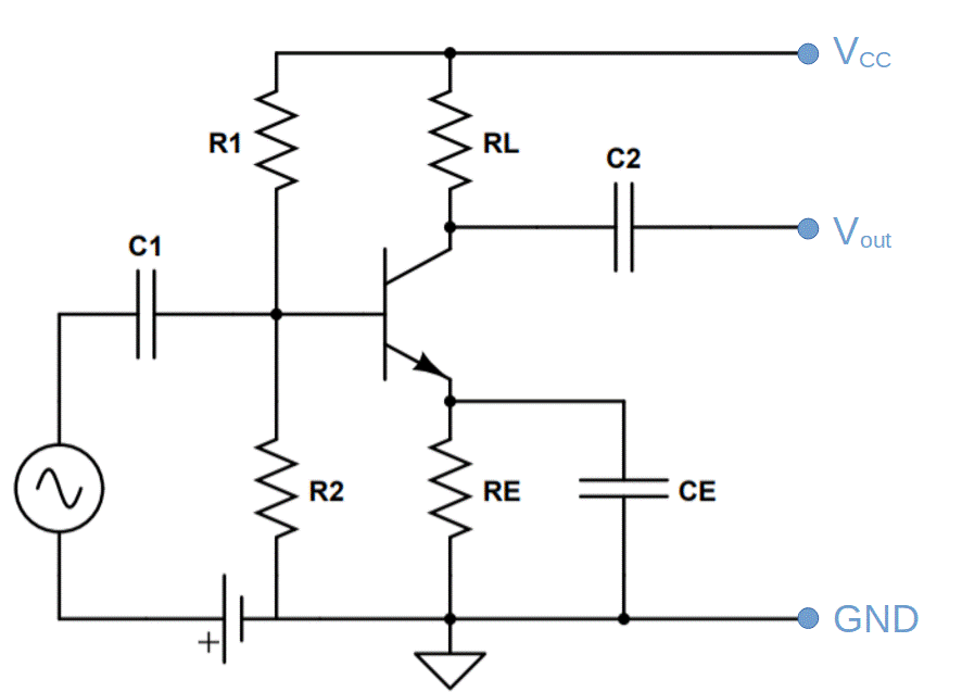
Coupling capacitors make use of the fact that capacitors block steady-state DC while allowing AC to pass. This can be understood in terms of frequency dependent capacitive reactance. The result is similar to a high pass filter on the input and output.
Capacitors must be carefully chosen to ensure that the circuit as a whole is optimized for the application frequency. Maximum output should be obtained over the desired frequency band.
A bypass capacitor on the emitter (CE) allows AC to bypass the resistor. DC will flow through the resistor to ground, while AC will preferentially flow through the bypass capacitor.