Semiconductors
Key Points:
- Semiconductors are materials that have a conductivity that is somewhere between that of insulators and conductors.
- The power of semiconductors is that they can be engineered through a process called doping.
- Doping allows us to make things like diodes and transistors out of semiconductors. These are the foundational building blocks of all electronics.
What Are Semiconductors?
Semiconductors are materials that not quite conductive. In other words, the conductivity of a semiconductor is somewhere between an insulator and a conductor.
If they don’t insulate and they don’t conduct, how are semiconductors useful?
It turns out that semiconductors are ideal materials to engineer electrically using a process called doping. Doping allows us to change the electrical properties of the semiconductor’s structure by adding atoms of other elements called dopants to the crystal lattice. For example, in silicon based devices, boron is commonly added to make a ‘p-type’ material, and phosphorous is often added to make an ‘n-type’ material. When you put a ‘p’ and an ‘n’ type materials next to each other, you obtain a ‘p-n junction’, the most fundamental building block of electronics.
Doping is so important that we’ve dedicated an entire lesson just to cover that topic. Without doping, semiconductors would still be pretty useless.
The amazing thing about doping is that we can develop devices that rely on new principles to function; we can make new types of devices. For instance, doping allows the development of really small diodes and transistors, which are like ‘neurons’ in the microprocessor ‘brain’. These developments would not have been possible without semiconductor doping.
The Information Age, aka The Silicon Age
You probably know that most semiconductors today are based on silicon. You might be wondering ‘what is silicon and why is it so important’?
Silicon is the second most abundant element in the earth’s crust, which is about 28% silicon by mass. The most common naturally occurring form of silicon is silicon dioxide (SiO2), which is also known as silica. In its natural mineral form, silica is called quartz, which probably constitutes most of the sand at your favorite beach.
How does silicon get from a surfside bar into computers? The answer, of course, is a lot of R & D.
Early semiconductor devices were not silicon based. The first semiconductor devices were actually based on the natural mineral lead sulfide (PbS), also known as galena. By the mid-20th century, scientists were primarily investigating the semiconductor germanium, which was used in radar systems during World War II. Like research into nuclear physics, WWII was a catalyst for scientific progress in semiconductors. The war effort resulted in the ability to create high quality germanium crystals and a good understanding of germanium doping (we’ll learn a lot about doping in this module). Thanks to these efforts, the first transistor was created in 1947 by John Bardeen and Walter Brattain, who were part of Bell Labs’ solid state physics group led by William Shockley.
Germanium remained the semiconductor of choice for another decade. In the late 1950’s, Bell Labs engineer Mohamed Atalla discovered that the surface of silicon could be passivated using oxygen or water at high temperatures. The passivation process forms an insulating layer of SiO2 that all but eliminated the hurdles of working with silicon. New devices made with silicon surpassed the performance of germanium-based devices. Given the abundance of silica on the earth, the industry quickly shifted from germanium to silicon as its’ material of choice.
Silicon is still the reigning champion that is used in most electronic devices. In order to make things like a computer processor, engineers take a sample of silicon and use microfabrication techniques to build the processor into/onto the silicon material.
In order to start tackling the basics of semiconductor devices, we’ll need to arm ourselves with some new tools that we haven’t yet encountered in this course. We’ll need to learn about the basics of semiconductor physics.
Semiconductor Crystal Structure
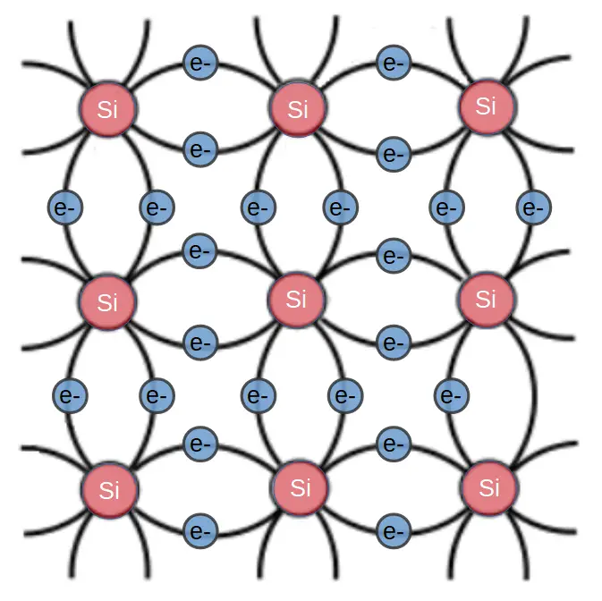
Semiconductors have crystalline structures. This means that the atoms in a semiconductor are form an ordered, periodic structure. Within a given crystal, we can predict where all the atoms are because silicon forms a basic pattern that is repeated over and over to form the whole crystal.
In a silicon crystal, each atom shares two electrons with four neighbors. In order for silicon to conduct, one of these bonds must be broken, resulting a ‘free’ electron. This electron is free to roam around the crystal or to participate in electric current.
When the electron leaves its’ atom, it leaves behind a (positively charged) electron hole.
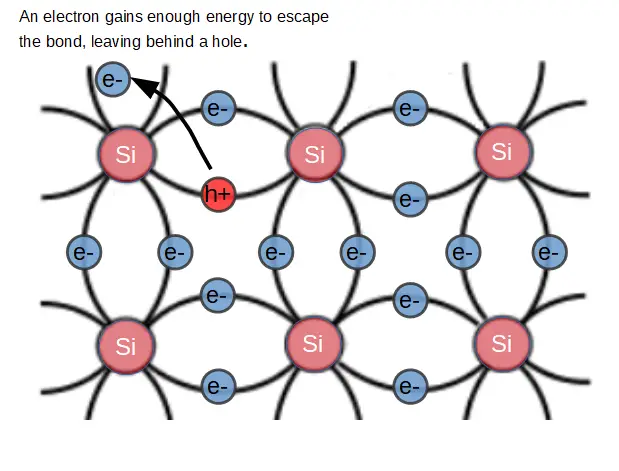
Holes are important concepts, and we’ll cover them in much more depth.
The important thing is to realize that semiconductors have crystalline structures, and that this crystal structure is responsible for how semiconductors behave.
Introduction to Semiconductor Physics
So far, we have learned about devices like resistors, capacitors, and inductors. Essentially, we have been concerned with controlling the flow of electrons using a combination of resistance, capacitance, and inductance.
Semiconductor devices are different. They control the flow of electrons by engineering the structure of the semiconductor crystal. In order to understand how this works, we have to learn some new tricks that will first be introduced in this lesson.
Electron Holes
Just like non-semiconductor devices, we are still primarily concerned with the flow of electric charge. In semiconductors, we are still interested in the behavior of electrons but we have have a new charge carrier: the electron hole. A hole is really just an empty ‘state’ that is left behind when an electron leaves an atom. They are not ‘real’ physical entities, but they help us to simplify the physics of semiconductors.
Band Diagrams
Another important tool is the semiconductor band diagram. In conductors, there is a plentiful amount of electrons that are free to conduct electricity. In insulators, there are zero electrons available to conduct electricity. We learned a rough model of why this is the case in our lesson on electric properties, but band diagrams will help us understand this much better. Band diagrams show us why conductors conduct, why insulators insulate, and why semiconductors…are somewhere in between.
In a semiconductor, it takes a little bit of energy to get some electrons to conduct. In its’ native state, without any applied energy, a semiconductor is basically an insulator. However when energy is applied in the form of heat, light, or voltage, some of the electrons are given enough energy to start conducting.
A band diagram is a useful representation of how electrons and holes behave in any given semiconductor material.
Semiconductor Band Diagram
Band diagrams are really useful to help understand a material’s electrical properties.
Let’s look at band diagrams for insulators, metals, and semiconductors in order to see how they work.
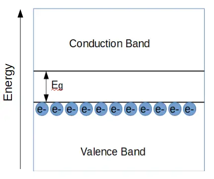
Band Diagram of an Insulator
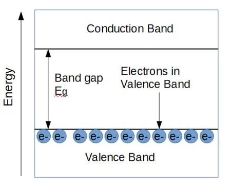
Band diagrams show the relationship between the ‘valence band’, which is the energy of the electrons in the valence shell, and the conduction band, which is the energy required to conduct electricity. Electrons in the valence band aren’t ‘free’ to conduct electricity; only electrons in the conduction band can conduct. In order for a material to be conductive, electrons must be in the conduction band.
In an insulator, the conduction band and valence band have a wide energy gap between them, called the band gap (Eg). The band gap is the energy needed for any electron to conduct electricity. In other words, if an electron absorbs energy (from light, heat, or voltage) that is greater than Eg, it can ‘jump’ up from the valence band into the conduction band, where it can contribute to electrical current.
In an insulator, the gap is so large that no electrons can conduct electricity. It would take a huge amount of energy to cause an insulator to conduct because the band gap is so large. If we give an insulator enough energy to force it to be conductive, we usually end up destroying the material in the process.
Band Diagram of a Semiconductor
Now let’s look at the band diagram of a semiconductor.
In a semiconductor, the band gap Eg is much smaller than the band gap of an insulator. It takes much less energy for an electron to enter the conduction band and conduct electricity. Let’s see how this works.
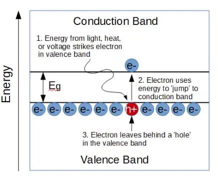
it ‘jumps’ up to the conduction band.
In a semiconductor, the energy band gap Eg is relatively small. Electrons that are in the valence band can absorb some energy from things light heat, light, or an applied voltage.
When an electron absorbs energy that is equal or greater than Eg, that electron can ‘jump’ up to the conduction band, where it may now contribute to electrical conduction.
The electron leaves an empty ‘state’ behind in the valence band. In other words, there is a hole where the electron used to be. It turns out that holes contribute significantly to semiconductor behavior.
We learned earlier that holes are created when an electron leaves its’ parent atom, leaving behind a positively charged ion. The band diagram shows the same thing, only it does so with more mathematical rigor. In both cases, the electron has absorbed enough energy that it now has more energy than the attractive force of the ‘potential well’ holding it in its’ bond.
Band Diagram of a Conductor
Band diagrams of conductors are useful to develop an intuition of how band diagrams can be used to understand electrical properties of all sorts of materials.
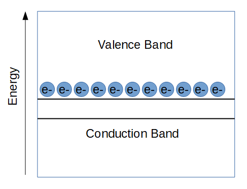
In a conductor, the valence band is actually higher than the conduction band. Unlike insulators and semiconductors, there is no band gap that electrons need to jump in order to be able to conduct. That’s why it doesn’t take any energy to get a conductor to conduct electricity.
Semiconductor Charge Carriers: Electrons and Holes
When we began learning about electricity, we discovered that electrons are at the heart of all electrical phenomena. When we say that something is conducting electricity, what is physically happening inside the material is that electrons are being pushed around.
When we enter the realm of semiconductors, electron holes become important as well. We saw in Figure 2 that holes are empty states that are left behind when an electron leaves its’ parent atom.
In terms of the atoms in the crystal, the electron can now leave it’s atom and participate in conduction. When it leaves the atom, it leaves behind a hole that another electron can jump into.
While holes are really just empty states, it can sometimes be much easier to talk about holes than about the electrons. If you think about a hole ‘moving’ through a crystal, of course what’s really happening is that electrons are just moving into the state occupied by the hole, leaving behind a hole at the state that the electron just came from. But thinking about things this way can be difficult.
A good analogy is that of a bubble floating in the air. When we think about the bubble, we consider it as it’s own entity; it’s obvious that the bubble is floating around. We don’t think about the bubble in terms of the air molecules around the bubble that are jumping out of the way for the bubble to move and jumping into the space occupied by the bubble right before it moves.
In the same way, it can be really useful to think about electron holes rather than the collection of electrons moving into an empty state and leaving behind an empty state, soon to be occupied by a different electron.
Intrinsic and Extrinsic Semiconductors
We saw earlier that one of the most important characteristics of semiconductors is our ability to add dopant atoms to the crystal lattice structure.
A semiconductor that is not doped (i.e. ‘natural’) is called an intrinsic semiconductor.
A semiconductor that is doped is called an extrinsic semiconductor.
There are two types of extrinsic semiconductors, which we saw briefly in our introduction: n-type semiconductors and p-type semiconductors. N-type semiconductors are known as donors, and p-type semiconductors are known as acceptors.
N-type Semiconductors
N-type semiconductors are doped with atoms that have one more valence electron that the semiconductor substrate. For example, phosphorous is often added to silicon to make an n-type material. Only a small amount of phosphorus is added so that each phosphorous atom is surrounded by many silicon atoms.
Silicon is in group 14 on the periodic table of elements, and has 4 valence electrons. Phosphorous is in group 15 and has 5 valence electrons- one more than silicon.
When a phosphorous atom is added to a silicon crystal, it bonds the same way silicon does- forming 4 bonds with the silicon atoms around it. Since phosphorous has 5 valence electrons and silicon only has 4, there is an extra electron from the boron atom, close to the atom but weakly bonded to it. The extra valence electron requires very little energy to jump to the conduction band and leave the atom. The electron is ‘almost’ free to conduct electricity.
N-type semiconductors therefore contribute ‘extra’ electrons that can participate in conduction. Dopant atoms (like boron) are called donors because they donate electrons to the silicon crystal.
P-type Semiconductors
P-type semiconductors are doped with atoms that have one less valence electron than the semiconductor substrate. For example, boron is in group 13 and has 3 valence electrons- one less than silicon. The boron atom is essentially ‘missing’ an electron when it is added to a silicon crystal. Each boron atom thereby contributes one hole state that a neighboring electron can easily occupy.
P-type semiconductors have many ‘extra’ holes that contribute to conduction. P-type dopant atoms (such as the Boron atoms added to the crystal) are therefore known as acceptors (because they accept electrons).
Extrinsic semiconductors are essential to the functionality of semiconductors. A diode is essentially a piece of n-type material next to a piece of p-type material, and a transistor can be made by adding a third piece, i.e. ‘NPN’ or ‘PNP’ transistors.
Conductivity of Intrinsic Semiconductors
Just as with metals and insulators, conductivity is an important concept when it comes to semiconductors.
In most materials, the conductivity (σ) is equal to the number of electrons (n), times the charge of a single electron ( |e| = 1.6 x 10⁻¹⁹ C), times the electron mobility (μe) of that particular material:
\sigma = n|e|\mu_e
In semiconductors, however, we don’t just have electrons to deal with anymore. We have to account for current due to holes, as well.
The formula is similar. Instead of ‘n’ representing the number of ‘negative’ charges (electrons), we now have ‘p’, representing the number of ‘positively’ charged holes. The |e| terms stays constant, as the value of each charge is the same. Instead of electron mobility (μe) we use hole mobility (μh).
The total conductivity of a semiconductor is the sum of the two terms, one for electrons and one for holes:
\sigma = n|e|\mu_e + p|e|\mu_h
In an intrinsic (un-doped) semiconductor, the total number of electrons is equal to the total number of holes (i.e. n = p). So we can simplify further.
\sigma = n|e|(\,u_e + \mu_h)
or
\sigma = p|e|(\mu_e + \mu_h)