741 Op Amp
The 741 op amp is one of the most popular op amps of all time. It is an integrated circuit (IC) that features low cost, high reliability, and good performance characteristics. It was one of the first op amps with features leading to widespread adoption over the following decades, and continues to be popular today.
Overview of The 741 Op Amp
An operational amplifier (often referred to as Op Amp) is a type of circuit that is complex and composed of resistors, capacitors, transistors and diodes.
The 741 operational amplifier, like other op amps, is a high gain voltage amplifier. It has many applications and has been extremely popular since its creation in 1968.
Op amps are a basic block in analog circuits and computers, where they are used to perform different types of analog signal processing tasks, mathematical operations in several linear, nonlinear, and frequency-dependent circuits.
The 741 operational amplifier is most commonly used in various electrical and electronic circuits. The main intention of this operational amplifier is to enhance AC and DC signals and for mathematical operations.
History of the 741 Operational Amplifier
Operational amplifiers were originally developed during the electron tube era and were used in analog computers. As transistor-based circuits grew in popularity, op amps also made the leap from tube-based to transistor-based construction. Generic operational amplifiers are available and popular as integrated circuits, in spite of the fact that discrete component versions are available for specific applications.
The first mass-produced Op Amp was the vacuum tube-based K2-W from GAP/R in January 1953. The first widely available integrated circuit op amp in the late 1960s was the Fairchild μA709 bipolar operational amplifier, created by Bob Widlar in 1965. In 1968, the μA709 was replaced by the μA741, which offered better performance while being more stable and easier to setup.
Although offering similar performance to its main competitor the LM101 from National Semiconductor, the μA741 became a standard because it had internal compensation capability making the μA741 easier to use than the LM101.
Over the decades, the 741 has remained an extremely popular chip. Nearly all manufacturers produce a variant of the 741, and it is a staple in circuit design, finding its way into many electronic products.
741 Op Amp Pin Out
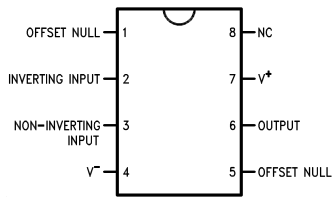
Power Pins 4 and 7
Pins 4 and 7 are the negative and positive voltage supply terminals. The power required to operate the integrated circuit comes from these two pins. The voltage level between these pins can be between 5 and 18V.
Output Pin 6
The output signal that is provided by the 741 Op Amp is received from this pin. The output voltage received on this pin is based on the feedback approach used and the voltage level on the input pins. When the voltage value on pin 6 is high, it means that the output voltage is similar to the supply voltage V+. Similarly, when the voltage value on pin 6 is low, it means that the output voltage is similar to the supply voltage V-.
Input Pins 2 and 3
These are the input pins of the operational amplifier. Pin 2 is considered the inverting input pin, while pin 3 is considered the non-inverting input pin. When the voltage value at pin 2 is greater that the value at pin 3, which means the inverting input has a high voltage value, the output signal is driven low. Similarly, when the voltage value at pin 3 is greater than the value at pin 2, which means the non-inverting input has a high voltage value, then the output signal is high.
Zero Offset Pins 1 and 5
As mentioned earlier, the 741 operational amplifier has an increased voltage gain level. For this reason, even small variations in the voltages at the non-inverting and inverting inputs, which occur due to anomalies in the construction procedure or other anomalies, will impact the output. To fix this, an offset value of the voltage is applied to pins 1 and 5, and this is usually achieved by a potentiometer.
Not Connected (NC) Pin 8
This is just a pin that is used to fill the empty pin of the 741 operational amplifier. It has no connection to any of the internal or external circuits.
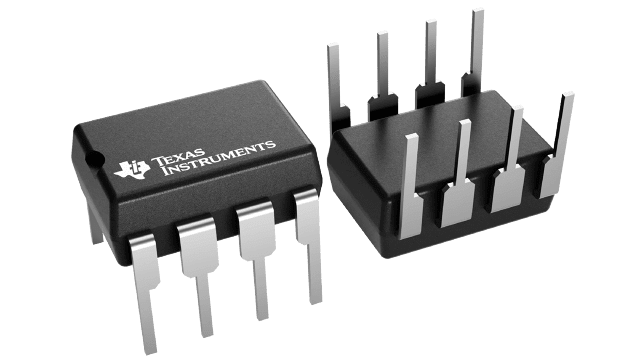
741 Op Amp Packages
An integrated circuit package is a housing that serves both an electrical junction and a mechanical interface between the integrated circuit chip and the printed circuit board. It is usually made of plastic, sometimes of ceramic, rarely of metal.
The different packages available for 741 Op Amp are:
TO99-8: an 8-pin round metal package with a body size of 9.08 mm × 9.08 mm.
SOIC-8: 8-pin flat package in which the direction of the pins is parallel to the substrate mounting surface.
CDIP: an 8 pin DIP (Dual In-line Package) package, and it is a type of ICs package where the pins go through the holes in the printed circuit board. This package has a body size of 10.16 mm × 6.502 mm.
PDIP: an 8 pin DIP package with a body size of 9.81 mm × 6.35 mm.
DIP-14: this DIP package has 14 pins total, 7 pins on each side.
How the 741 Op Amp Works
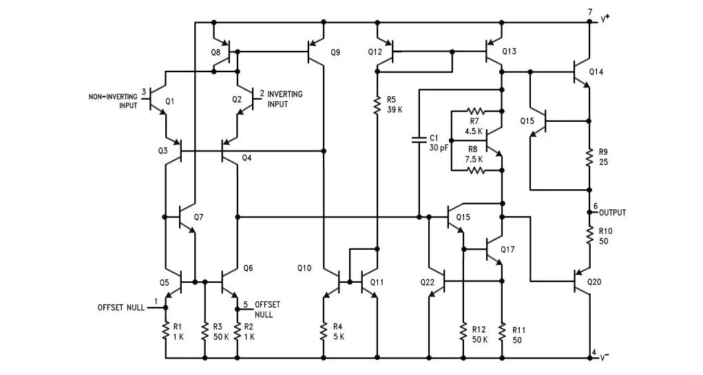
Internal schematic of 741 operational amplifier
For transistors Q1 and Q2, the inverting and non-inverting inputs are connected in correspondence. Transistors Q1 and Q2 work as NPN emitters where their outputs are connected to the pair of transistors Q3 and Q4 which work as common base amplifiers. This type of configuration isolates the inputs that have a connection to Q3 and Q4 and thus eliminates the signal feedback that could occur.
Voltage fluctuations that occur at the inputs of the operational amplifier can impact the current flow of the internal circuit and also impact the effective functional range of any transistor that is in the circuit. So, to prevent this from happening, there has been the implementation of two current mirrors. The pairs of transistors (Q8, Q9) and (Q12, Q13) are connected to form mirror circuits.
Since transistors Q8 and Q12 are the regulating transistors, they set the voltage level at the EB junction for their corresponding pair of the transistor. This voltage level can be set precisely to a few decimal places of millivolts, and this precision allows only the necessary current flow to the circuit.
One mirror circuit which is composed of Q8 and Q9 is fed to the input circuit while the other mirror circuit composed of Q12 and Q13 is fed to the output circuit. In addition, the other mirror circuit which is the third one formed by Q10 and Q11 works as an increased impedance connection between the V- supply and the input. This connection provides a reference voltage level showing no load effect on the input circuit.
Transistor Q6 along with the 4.5K and 7.5K resistors are a voltage level shifter circuit that decreases the voltage level of the amplifier circuit at the input section by Vin before it is passed to the next circuit. This is done to eliminate any kind of signal variations at the output amplifier section. While transistors Q22, Q15 and Q19 are designed to operate as a Class A amplifier, and transistors Q14, Q20 and Q17 are the output phase of the 741 Op Amp.
In order to eliminate any type of anomalies at the input phase of the differential circuit, transistors Q5, Q6 and Q7 are then used to form a configuration that has zero +Vin and -Vin offset and inverting and non-inverting input levels accordingly.
741 Op Amp Specifications
Here is a table giving the characteristics of the 741 operational amplifier:
| Property | Value | Unit |
| Amplification A | 2 * 105 | – |
| Gain G = 20.log(A) | 106 | – |
| Input impedance | 2 * 106 | Ω |
| Output impedance | 75 | Ω |
| Cut-off frequency | 10 | Hz |
| Leakage currents I+, I- | 80 * 109 | A |
| Offset voltage | 1 * 10-3 | V |
| Common-mode rejection ratio (CMRR) | 90 | dB |
741 Op Amp Input Impedance
The input impedance of an operational amplifier is determined by its input transistors. The input of an Op Amp can be modeled by three resistors: two common mode resistors and a differential resistor. The common mode resistors are connected between one of the two inputs and zero while the differential resistor is arranged between the two differential inputs. These resistors have values between 105 and 1012 Ω depending on the technology of the transistors used.
741 Op Amp Output Impedance
The output impedance of an operational amplifier is not zero. It is between 50 Ω and 200 Ω. This output impedance results in a drop in the output voltage as the load current increases. In a circuit using negative feedback, the output impedance is divided by the gain of the feedback loop, which brings it to a value close to zero.
Offset Voltage of the 741 Op Amp
The offset voltage of an operational amplifier is a parasitic DC voltage that originates due to the difference between the input voltages. It results from small asymmetries between the characteristics of the internal or external components of the two inputs. This is because circuit components can not be made perfectly identical. In practice, this results in an “unexpected” shift of the output voltage.
The offset voltage is directly amplified by the circuit. On ICs with a zero setting, this offset can be canceled by connecting a potentiometer to the appropriate pins. If the operational amplifier is not equipped with zero adjustment pins, it is necessary to use an external circuit to cancel this offset. This way of doing things also makes it possible to get rid of the differences in the offset adjustment mode provided by the manufacturers according to the type of the operational amplifier, and thus to improve interchangeability.
It is worth mentioning that, whatever the method of offset compensation chosen, the offset of these ICs varies with its temperature and some methods can increase this variation or even cancel it.
741 Op Amp Common Mode Rejection Ratio
The common mode rejection ratio (CMRR) is a numerical value that represents the ability of an operational amplifier to reject the common voltage of its two inputs. It is usually expressed in decibels (dB).
In practice, the output voltage of an Op Amp does not only depend on the voltage difference between the two inputs. It also depends on the average value of the voltages on these two inputs (or common mode voltage).
In general, the CMRR in direct current (DC) varies between 70 and 130 dB depending on the type of amplifier, but it decreases significantly with the increase of frequency.
Applications of the 741 Op Amp
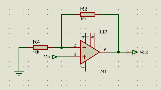
741 Op Amp Inverting Amplifier
This arrangement allows to amplify the signal at the input by the gain A and inverting it. The value by which we multiply the input voltage to obtain the output voltage is calculated by dividing the value of the resistor R2 by R1 with the sign – because the signal is inverted.
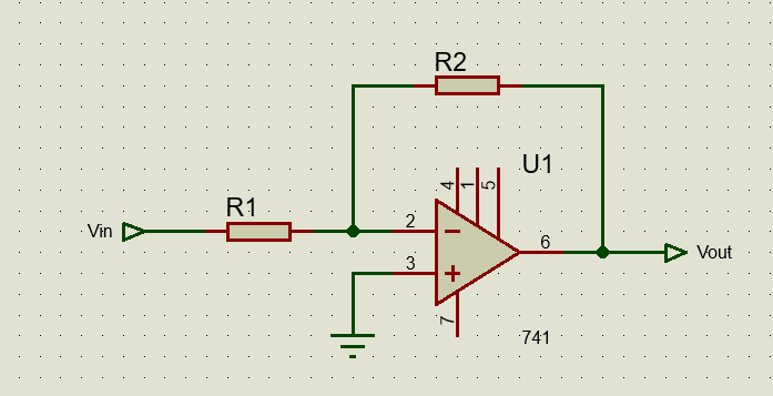
Inverting amplifier circuit using 741 Op Amp
741 Op Amp Non-Inverting Amplifier
This arrangement allows to amplify a signal by the gain of the circuit.
Non-inverting amplifier circuit using 741 Op Amp
741 Op Amp Voltage Follower
The 741 can be used to construct a voltage follower, also known as a buffer.
In this arrangement, the value of the input signal follows that of the output signal. This circuit may seem useless because the gain A = 1, but it is very practical in the case where we have an input signal with a certain level of voltage but a low current. At the output of the amplifier the voltage will be preserved but we will then have the current necessary to control the rest of the circuit.
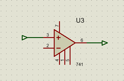
Voltage follower circuit using 741 Op Amp
741 Op Amp Inverting Summing Amplifier
As its name indicates, the adder is a circuit whose output voltage is equal to the sum of the voltages applied to each of its inputs. In this configuration, the summing amplifier will invert the signal as well as performing the adding function.
The name “mixer” applies to the circuit that “mixes” alternative signals, it is widely used in audio.
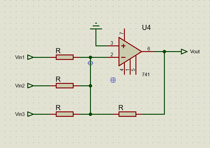
Inverting summing amplifier circuit using 741 Op Amp
741 Op Amp Differential Amplifier or Voltage Subtractor
This circuit allows to amplify the difference of two signals. It is used as a comparator between 2 voltages Vin1 and Vin2 and also as a regulator.
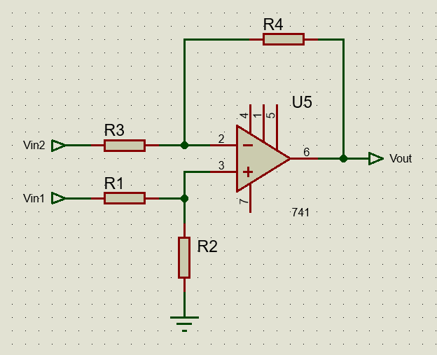
Differential amplifier circuit using 741 Op Amp
741 Op Amp Filters
741 Op Amp Second Order Low-Pass Filter
A low-pass filter is a filter that allows low frequencies to pass and attenuates high frequencies, i.e., frequencies above the cut-off frequency.
A second order low-pass filter is characterized by its natural frequency (often referred to as f0) and by the quality factor or Q factor which is defined as the ratio of the resonant frequency to the bandwidth.
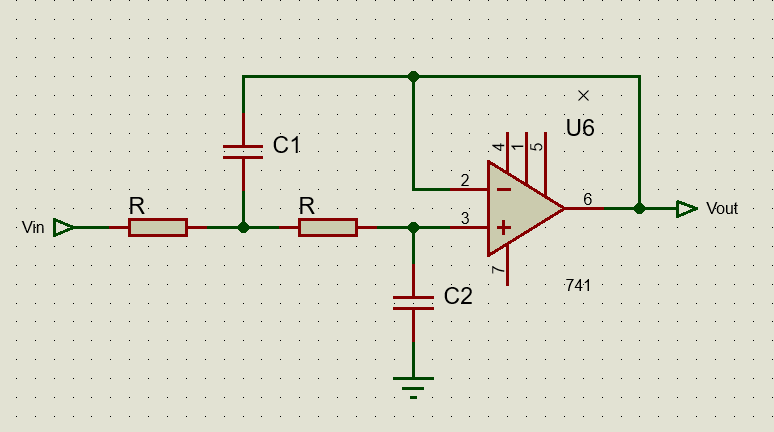
Second order low-pass filter circuit using 741 Op Amp
741 Op Amp Second Order High-Pass Filter
A high-pass filter is a filter that allows high frequencies to pass and attenuates low frequencies. It could also be called a low-cut filter. The high-pass filter is the inverse of the low-pass filter and these two filters combined form a bandpass filter which allows only a defined range of frequencies to pass.
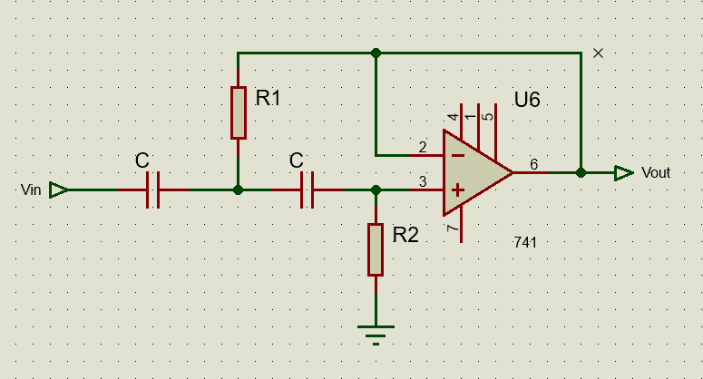
Second order high-pass filter circuit using 741 Op Amp
741 Op Amp Non-linear applications
Schmitt Trigger using the 741 Op Amp
The regenerative comparator, also called Schmitt Trigger, reconstitutes a hysteresis cycle. The -Vin terminal is used as reference, but this one varies according to the output to which it is connected by the voltage divider (R1 and R2). As the reference varies, we avoid an intermittent operation as the output switches from one state to the other in a less close way.
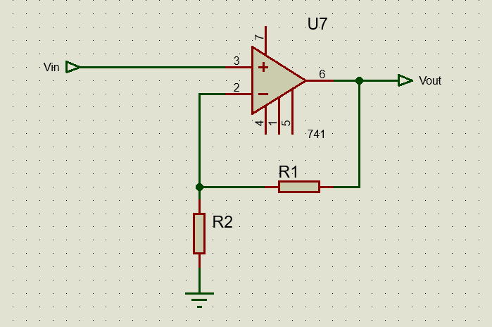
Schmitt trigger circuit using 741 Op Amp
741 Op Amp Circuits and Projects
Automatic Night Light using the 741 Op Amp
This is a simple project using an LM741 operational amplifier and a photoresistor to detect light or darkness.
A photoresistor is connected to pin 2 which is the inverting input of the operational amplifier, an LED is connected to the output pin (pin 6) to indicate the absence or presence of light and a variable resistor that allows to adjust the circuit sensitivity is connected to pin 3.
The way the circuit is connected it forms a light sensor. In a dark room reasonably, the light is off. A bright light on the photoresistor will cause the LED to light up. If you reverse the wires going to pins 2 and 3, it will be a darkness detector. In the dark, the light will be on, and a bright light on the photoresistor will cause the LED to turn off.
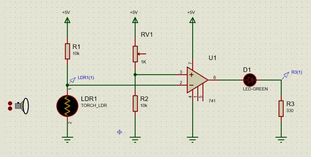
Automatic night light circuit using 741 Op Amp
Hartley Oscillator with 741 Op Amp
The Hartley oscillator is distinguished by an LC circuit consisting of two inductors connected in series in parallel with a capacitor, with an amplifier between the relatively high impedance of the entire LC circuit and the relatively low voltage or current point between the inductors.
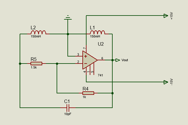
Hartley oscillator circuit using 741 Op Amp
741 Op Amp Power Regulator
This power regulator is composed of the operational amplifier LM741 and a couple of power transistor (ex: 2N3055). It receives a voltage of 12V to 30V at the input and puts out a fixed voltage of 10V at the output with a maximum output power of 10A.
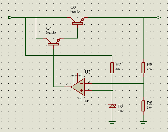
Power regulator circuit using 741 Op Amp
Alternatives to the 741 Operational Amplifier
TL081
The TL081 operational amplifier has the advantage of having a very high input impedance (Field-Effect Transistors). On the other hand, it has the disadvantage of not accepting input voltages lower than 2V above their negative supply, and only being able to produce an output voltage within a range of 2.5V below the supply voltage limits. These specifications do not allow this operational amplifier to be supplied with voltages lower than ±5V (i.e., 10V unbalanced).
| Property | Value | Unit |
| Amplification A | 2 * 105 | – |
| Gain G = 20.log(A) | 106 | – |
| Input impedance | 1012 | Ω |
| Output impedance | 100 | Ω |
| Cut-off frequency | – | Hz |
CA3140
The CA3140 is a BiMOS (an integrated circuit technique combining the advantages of CMOS and bipolar in a single integrated circuit) operational amplifier where the input stage consists of MOS field effect transistors (MOSFET).
| Property | Value | Unit |
| Amplification A | 105 | – |
| Gain G = 20.log(A) | 100 | – |
| Input impedance | 1.5 * 1012 | Ω |
| Output impedance | 60 | Ω |
| Cut-off frequency | ~ 20 | Hz |
LMC6035
The LMC6035 operational amplifier is a LinCMOS (Linear zone CMOS) IC made up of CMOS transistors operating in the linear zone and it offers extremely high input impedance and ultra-low bias.
| Property | Value | Unit |
| Amplification A | 106 | – |
| Gain G = 20.log(A) | 106 | – |
| Input impedance | > 1013 | Ω |
| Output impedance | – | Ω |
| Cut-off frequency | – | Hz |
The 741 Op Amp – Conclusion
In conclusion, the 741 is an operational amplifier with a wide variety of applications. Its’ low cost, specifications, and packaging options, as well as its’ history within the industry, have led to the incredible success of the 741. These factors combined, have resulted in the 741 being one of the most popular integrated circuits of all time.