P-N Junction
What Are P-N Junctions?
A p-n junction is an interface between p-type and n-type semiconductor materials within a single semiconductor crystal.
One side of the junction is a p-type doped semiconductor, and the other side is an n-type doped semiconductor.
We learned in the last lesson that p-type and n-type semiconductors have distinct electrical characteristics, and that these characteristics can be understood by using a band diagram.
When p and n-type semiconductors are combined into a single unit (called a p-n junction), a new device is created that harnesses the power of both types of material. By itself, a p-n junction functions as a diode, the first semiconductor device that we’ll encounter in this course.
Just as importantly, p-n junctions form a critical, fundamental building block of almost all semiconductor-based devices including transistors like the metal oxide silicon field effect transistor (MOSFET)- the foundation of computer processors.
Most transistors are a variant of two P-N junctions that are placed back to back, either in a PNP or NPN configuration. Transistors can even be tested this way, by testing each side of the transistor by pretending that it is simply two separate P-N junction diodes.
How P-N Junctions Work
P-N junctions are what you get when you combine a p-type semiconductor and an n-type semiconductor, back to back, in a single crystal, with no boundaries between them.
It might seem simple, but some surprising things happen as a result. Let’s take a look at a p-n junction to learn how they work.
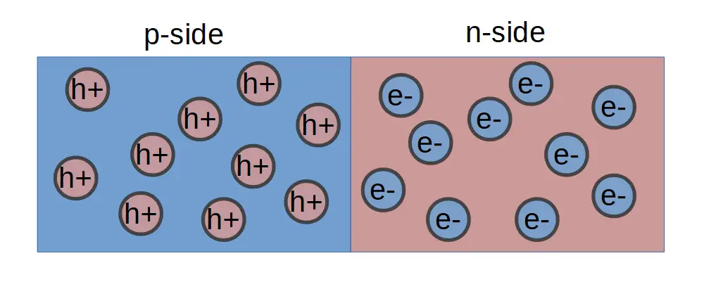
The p-side contains a plethora of free holes and the n-side contains free electrons. Both sides are electrically neutral, as the charged atoms (ions) on either side balance out the charge of the free electrons and holes.
On the p-side of the junction, negatively charged ions balance the charge of the free (positively charged) holes. On the n-side, positively charged ions balance the charge of the free (negatively charged) electrons.
P-N Junction With No Bias
Some interesting things occur before we even place a voltage across the P-N junction. Almost immediately, the situation changes so that we no longer have a simple p-doped section next to an n-doped section.
Since the p-side has free holes that are positively charged and the n-side has free electrons that are negatively charged, there is an attraction between the holes on the p-side and electrons on the n-side.
The holes move right toward the center of the junction, and the electrons move to the left.
When the electrons and holes meet in the middle, a phenomenon called carrier recombination takes place.
The free electrons and holes that meet in the center combine with a release of energy (this is how LEDs produce light).
This process happens almost instantaneously, right after the P-N junction is made on the assembly line. The result is that the p-n junction features two areas that are now electrically charged. These two areas are together called the depletion region because there are no free charge carriers left within the region.
The right edge of the p-side is the negatively charged area of the depletion region. It has negatively charged ions (i.e. atoms with an extra electron) because the positively charged holes have been destroyed during carrier recombination. Without the free holes to keep it neutral, there is a negative charge in this area.
Similarly, the left edge of the p-side now has positively charged ions because the atoms in the N-side of the depletion region have lost their electrons.
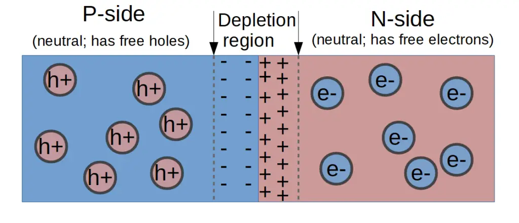
All of this happens very quickly so that this is the ‘starting position’ of a p-n junction. The two sides and depletion region in the middle dictate how the p-n junction will behave when we place a voltage across it.
Forward and Reverse Bias
We’ve seen that a direct current (DC) power source has a positive and negative terminal. A direct current flows from the positive terminal through the circuit to the negative terminal. There are therefore two ways that we can connect a p-n junction to the circuit.
We can connect the p-side to the positive terminal and n-side to the negative terminal, which is called forward bias.
Or we can connect the p-side to the negative terminal and the n-side to the positive terminal, which is called reverse bias.
You may have heard that diodes only allow current to pass in one direction, which is called rectification. All diodes have this feature, including the simplest diode, which is simply a p-n junction (technically this type of diode is called a ‘p-n junction diode’). This feature is used to convert AC to DC or to prevent current from ‘accidentally’ sneaking in the wrong direction and damaging something.
P-N Junction with Forward Bias
Forward bias is achieved when a p-n junction is placed with the positive terminal of the power source on the p-side and negative terminal on the n-side.
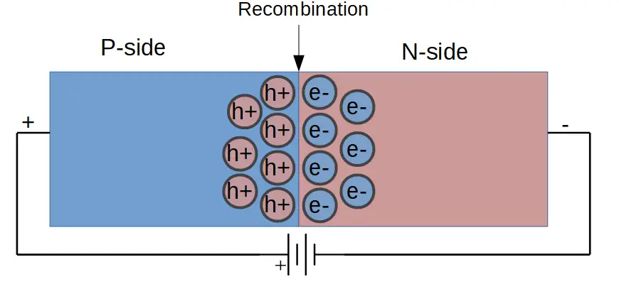
In this configuration, current flows from the positive terminal as it does in any other circuit. When the current reaches the p-side, it pushes the holes (right) toward the middle of the junction. This is because the (positively charged) holes are repelled by the positive charge at the positive terminal of the power source.
At the same time, electrons flow out of the negative terminal of the power source through the side of the circuit leading to the n-side of the p-n junction. When these electrons reach the n-side of the p-n junction, they repel the free electrons in the n-side material. The electrons are pushed (left) toward the center of the junction. Another way of looking at this is that the electrons are attracted to the left by the current.
Electron-Hole Recombination
As the holes on the p-side are pushed rightward toward the center and the electrons on the n-side are pushed leftward toward the center, they begin to recombine.
This recombination action is how current works in a forward biased p-n junction. Within the p-n junction, holes and electrons recombine. However, the rest of the circuit is not impacted by the recombination within the junction. The rest of the circuit functions as normal.
The free electron is in the conduction band, and the free hole is in the valence band. Recall that the conduction band is at a higher energy than the valence band; in other words, the electron has more energy than the hole it combines with.
When the electron combines with the hole, what happens is that the high energy electron falls down to the energy level of the hole. That energy has to go somewhere, so it is released by the electron in the form of a photon, which is a particle of electromagnetic radiation, in the form of heat or light.
However, the action does not stop there! Holes are not ‘real’ particles; they are ways of modelling more complex electron movement. As holes move to the right, toward the center of the P-N junction, what is really happening is that electrons are jumping into empty hole states. In other words, a hole moving to the right corresponds with an electron moving to the left.
The electron may no longer be in the conduction band, but it can still move via the movement of holes through the p-side, and into the rest of the circuit.
When the electron reaches the end of the p-type, or the junction between the p-type material and the conductor (wire) it connects to, it doesn’t need to gain any energy to continue to conduct. This is because the valence band of the conductor is above the conduction band. The electron continues to contribute to current on its’ own, without the need for holes.
All of this takes place only when a P-N junction is forward biased.
In contrast, a p-n junction that is reverse biased cannot pass current. This is why diodes can be thought of as rectifiers, or ‘check valves’ for electric current.
P-N Junction with Reverse Bias
When a p-n junction is placed in the reverse bias configuration, the junction functions to stop the passage of current.
Instead of being pushed toward the center of the junction and recombining, the charge carriers (electrons and holes) migrate to the edge of each material and prevent current from passing through the junction.
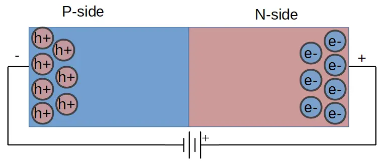
On the p-side, the free holes are now attracted to the negative charge supplied by the negative terminal of the power source. Thus the holes migrate to the left, away from the center of the junction.
On the n-side, the free electrons are attracted to the positive terminal of the power source. The electrons migrate to the right, away from the junction.
The junction itself is now relatively free of free charges; with no capability of producing new electrons or holes, it becomes insulative and prevents current from continuing to flow.
How Current and Electrons Flow in a Diode
With a forward bias applied, holes and electrons recombine at the center of the junction. But what is actually happening