Semiconductor Doping
Semiconductor doping refers to the addition of ‘dopant’ atoms to a semiconductor crystal in order to change the electrical properties of the crystal.
We start with a pure crystal of a semiconductor material, typically silicon. Every atom within the crystal is an atom of silicon. To change the electrical properties of the crystal, we add other (non-silicon) atoms to the crystal. These atoms are called dopants. Enough dopants are added to change the electrical properties, but not so many that the crystal structure itself is altered.
The dopant atoms function as either electron donors (called n-type) or acceptors (called p-type). Donors result in many free electrons that can contribute to electrical conduction. Acceptors result in a large amount of holes, which also contribute to electrical conduction by facilitating valence electron movement.
We learned in the last lesson that semiconductor doping is very important. Doping is essentially the reason that semiconductor devices are so popular today.
Virtually all commercially available semiconductor devices are doped, meaning that they are all extrinsic semiconductors.
Semiconductors don’t have to be highly doped in order to be effective. Just one dopant atom out of a huge number (about 1012) silicon atoms will give the silicon crystal extrinsic properties.
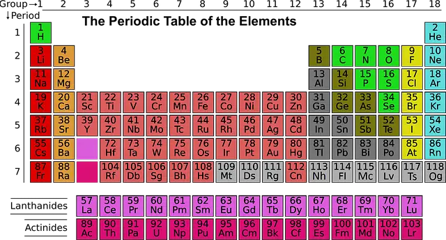
Semiconductor Doping and the Periodic Table
In order to better grasp the principle of doping, it is helpful to reference the periodic table of elements.
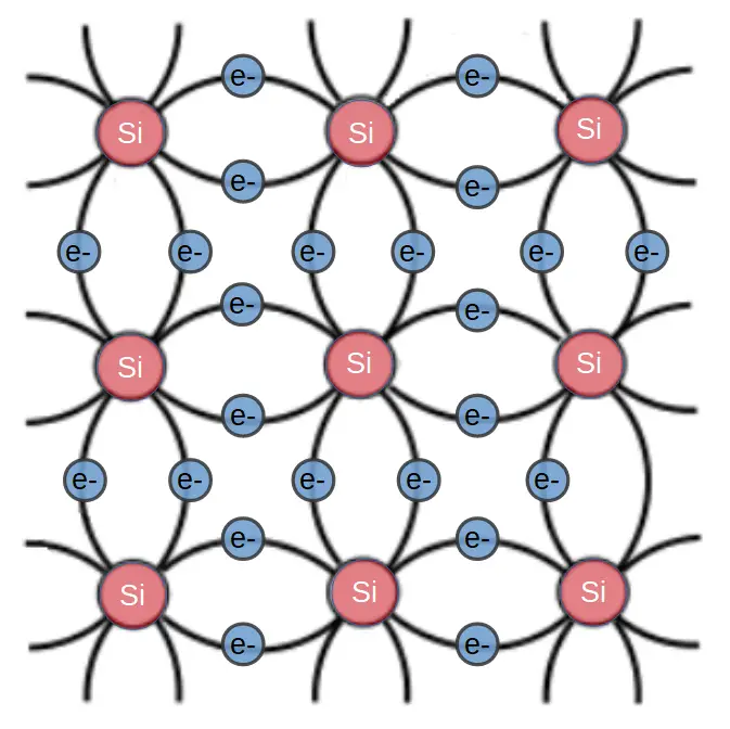
Silicon has an atomic number of 14, meaning that there are 14 protons in the nucleus of a silicon atom. A silicon atom has 14 electrons in its’ neutral state, 4 of which are in the outermost (valence) shell. In a silicon crystal, each of the 4 valence electrons are shared with a neighboring atom. This allows each silicon atom to covalently bond to four other silicon atoms, resulting in 4 double bonds because each atom shares an electron with its’ neighbors. This is symbolized by the two lines in between each silicon atom in the image below, each line indicating a chemical bond with a single shared electron.
In order to dope a silicon crystal, we have to introduce atoms that result in a weakly bonded electron or hole.
Since silicon has four valence electrons, if we want to create more free electrons, we have to dope with an atom that has more electrons than silicon itself. We therefore use atoms with 5 valence electrons, with the most common n-type dopants being phosphorous (P) and arsenic (As). This results in the formation of an n-type semiconductor, and the dopant atoms are referred to as electron donors.
If we want to produce a material that has more free holes, we have to dope with an atom that has less electrons than silicon. For this purpose we use atoms with 3 valence electrons. The most common p-type dopants are boron and aluminum. Dopant atoms in a p-type semiconductor are referred to as acceptors, because the holes that they generate can be easily occupied by neighboring electrons.
N-Type Semiconductors
The key to n-type semiconductors is that they have electrons that are weakly bonded to their parent atoms. At room temperature, there is enough ambient thermal energy to excite these electrons into the conduction band. Any electric field or voltage applied will then cause these electrons to conduct.
N-type semiconductors are produced by introducing dopant atoms that have one more valence electron than the semiconductor substrate. For instance, silicon has 4 valence electrons so n-type dopants such as phosphorous or arsenic have 5 valence electrons. These atoms are introduced into the crystal in a low enough concentration that they simply take the place of a silicon atom:
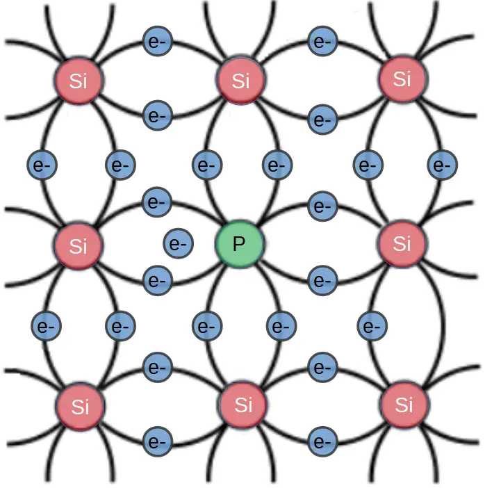
In an n-type semiconductor, dopant atoms function as electron donors. Each atom contributes one electron that is only weakly bonded to it’s parent atom. The energy state of this electron is based viewed with a band diagram.
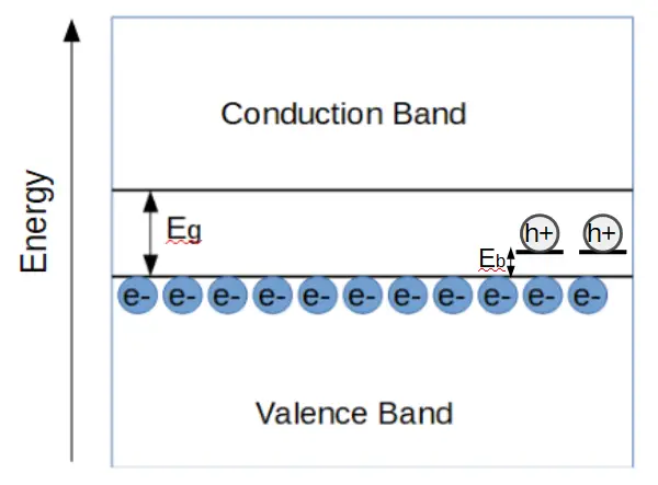
Band Structure of N-Type Semiconductors
The band structure of an n-type semiconductor is distinguished from an intrinsic (un-doped) semiconductor by the presence of states inside the band gap, close to the conduction band. These are shown as the two electrons just below the conduction band in the figure below. These electrons occupy states within the band gap; i.e. they are valence electrons that are not in the valence band. They have more energy than valence band electrons.
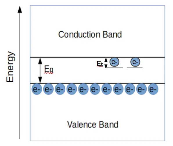
At room temperature, these electrons will jump up into the conduction band and will contribute to conduction if a voltage is applied. The new ‘states’ contributed by the dopant atoms are called donor states.
Unlike the electrons contributed by the silicon atoms, the electrons in donor states do not have to acquire enough energy to jump above the bandgap, Eg. Instead, they only have to acquire an energy Eb, short for bonding energy. Eb is generally less than the thermal energy available at room temperature. Therefore each dopant atom results in a donor state that provides one free electron at room temperature.
P-Type semiconductors
While N-type semiconductors contribute free electrons, p-type semiconductors contribute free holes.
A hole, or electron hole, is an unfilled state in the crystal that corresponds with an empty state in the valence band. Let’s review how holes are formed in intrinsic semiconductors to see how p-type semiconductors work.
Holes in Intrinsic Semiconductors
In an intrinsic (un-doped) semiconductor, a hole is formed when an electron leaves its’ parent atom behind. The electron absorbed enough energy to break the chemical bond holding it in place, and it will contribute to electric current if a voltage (electric potential difference) is applied across the semiconductor crystal.
When the electron leaves its’ atom, it leaves behind a positively charged ion and a state that can easily be occupied by another electron. In other words, there are two modes of conduction at work:
The first mode of conduction is the current that is contributed by the original electron, now in the conduction band.
The second mode of conduction is the movement of another, still-bonded electron from its’ own bond, into the hole that was made available by the first electron. This hole was left in the valence band, so electrons don’t need to acquire enough energy to reach the conduction band. When a voltage is applied across the crystal, the valence electrons will preferentially move as much as possible via available holes.
In an intrinsic semiconductor, the number of free electrons in the conduction band is equal to the number of holes in the valence band.
Holes in P-Type Semiconductors
In P-Type semiconductors, an electron does not need to be excited across the band gap in order to generate a hole.
Instead, a dopant atom that has one less valence electron than the atoms of the semiconductor crystal is used to create an ‘extra’ hole in the crystal.
For instance, boron is in Group 13 (also called Group 3A or Group IIIA) of the periodic table and has one less valence electron than silicon. When a small amount of boron atoms are added to a silicon crystal, the boron will arrange itself in the crystal as a replacement to a silicon atom.
But instead of boron sharing 4 sets of double bonds (like its’ silicon neighbors), it only has 3 electrons to contribute. There is an extra bonding state that is unfilled due to the lack of an electron. This extra bonding state functions as a hole that can be occupied by electrons in the valence band.
Unlike an intrinsic semiconductor, the number of free electrons and holes are not the same. In a p-type material, the number of free holes will vastly outnumber the quantity of free electrons.
Band Structure of P-Type Semiconductors
The band structure comes in handy once again in depicting the mechanism for hole conduction.
In a p-type material, new states are created just above the valence band. When an electron from the valence band is excited into the dopant state, the electron leaves an empty state behind in the valence band, i.e. a hole.
This hole contributes to conduction just as holes do in intrinsic materials. Although holes aren’t ‘real particles’, the effect of electrons conducting via jumping ‘into’ the vacant hole state is easily modeled by them. The hole is considered to have a positive charge, and moves in the opposite direction of electrons when a voltage is generated across the crystal.
The Effect of Semiconductor Doping on Conductivity
We have seen that the conductivity of an intrinsic semiconductor is the sum of the contributions from both electrons and holes.
In intrinsic semiconductors, the quantity of electrons is always equal to the number of holes.
In extrinsic semiconductors, the quantity of electrons is very different from the number of holes.
N-type semiconductors have more electrons that are free to conduct.
P-type semiconductors have more holes that are free to conduct.
In fact, n-type semiconductors have so many more electrons that their conductivity is roughly equal to the conductivity contributed by the electrons.
\sigma \cong n|e|\mu_e
Ans in p-type semiconductors, the conductivity is roughly equal to the contribution of the holes:
\sigma \cong p|e|\mu_h