Metal Oxide Semiconductor Field Effect Transistor (MOSFET)
MOSFETs (metal oxide semiconductor field effect transistors) are the most widely produced electronic component in history. They form the backbone of the modern computer industry, and their contribution to human civilization would be difficult to overstate. An estimated 13 sextillion (13 x 1021) MOSFETs had been produced by 2020.
A MOSFET is a semiconductor device that controls the flow of current by using a voltage signal to modulate the width of a conductive channel in the body of the transistor.
Like many other semiconductor devices, a MOSFET is usually made of doped silicon.
There are a few advantages of MOSFETs that have enabled them to become so popular. First, MOSFETs use voltage, rather than current, to control operation so power consumption is extremely low. They can also be scaled to incredibly small sizes (as predicted by Moore’s Law). As their size decreases, the average cost per transistor also decreases. These attributes make them perfect for use in integrated circuits like computer processors and memory.

Like other forms of transistors, MOSFETs can be used as a switch and as an amplifier. What makes them unique is that they use an electric field to control current; this means that other than a small amount of leakage current, MOSFETs don’t dissipate a significant amount of power in order to function. In addition, their simple design makes them perfect for scaling down to almost atomic sizes.
These attributes make MOSFETs perfect for use in computer applications. Over time, they have overtaken all other electronic components, becoming the most widely produced electronic component in history. This is primarily due to their use in logic circuits, where they perform the binary switching and memory storage operations in computer processors and memory.
What is a MOSFET?
MOSFET stands for metal oxide semiconductor field effect transistor. Within the long acronym of the name ‘MOSFET’ are two acronyms that describe what a MOSFET is.
Field Effect Transistor (FET)
The acronym FET describes a field effect transistor. An FET is a type of transistor that uses a field effect to control current flow. In other words, an electric field is used to control the flow of charge carriers by influencing them from a distance. There is a separation between the voltage that causes the field, and the charge carriers that contribute to current.
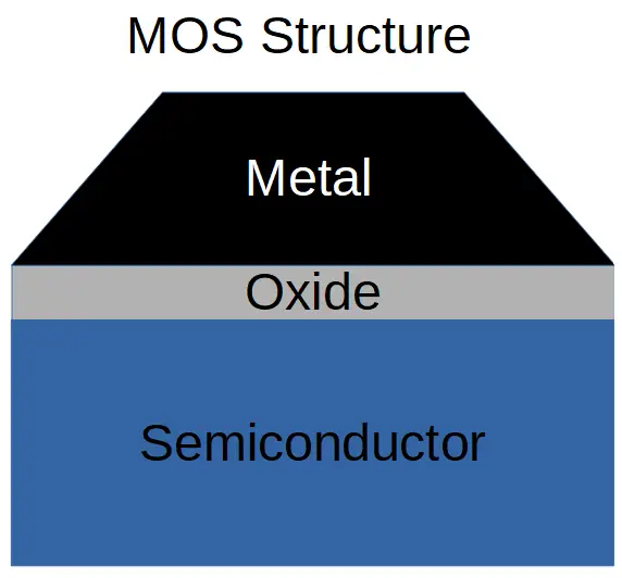
Metal Oxide Semiconductor (MOS)
The acronym MOS tells us how this separation is formed. MOS stands for metal oxide semiconductor, which describes a three layer system consisting of a metal, an insulating oxide, and a semiconductor.
The bottom of the structure is a semiconductor crystal that is usually lightly doped. The top of the crystal is oxidized by impregnating the semiconductor crystal with oxygen, which forms a polarizable electric insulator (i.e. a dielectric). Finally, a metal surface is deposited on top of the oxide to allow an electrical contact to be formed.
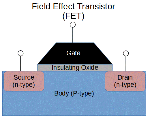
In terms of its’ construction, a MOSFET is comprised of an MOS structure that makes up its’ gate and body, with two heavily doped regions on either side. The MOS structure allows a bias on the metal to influence charge carriers in the semiconductor while each side is insulated from the other by the presence of an oxide.
Field Effect Transistor (FET) vs. Bipolar Junction Transistor (BJT)
We introduced the subject of transistors by first looking at the bipolar junction transistor (BJT). BJTs are a perfect starting point because they are directly based on two P-N junctions. Field effect transistors aren’t more complicated than BJTs, but it helps to understand the BJT first so that it can function as a reference.
Until this point, all of the semiconductor devices that we have covered have been based on the construction of P-N junctions. This includes diodes, LEDs, Zener diodes, and bipolar junction transistors.
Unlike these devices, FETs do not operate on the principle of the P-N junction (even though they have two P-N junctions like BJTs). Instead, minority carriers from the doped body of the transistor are attracted together by an electric field to form a channel through the body of the transistor. The channel allows conduction through the transistor.
Despite both devices being types of transistors, these two devices have different characteristics that make them good for different things. The following table provides a comparison of attributes.
| Bipolar Junction Transistor (BJT) | Field Effect Transistor (FET) | |
| Controlled by | Current | Voltage |
| Number of charge carriers | Two; both electrons and holes | One; either electrons or holes |
| Number of terminals | Three | Three or four |
| Impedance | Low | High |
| Power consumption | High | Low |
| Amplification | High | Low |
| Scalability | Low | High (can be made very small) |
| Cost (relative) | High | Low |
Structure of a MOSFET
MOSFETs have three terminals. These terminals are called the source, gate, and drain and correspond roughly to the emitter, base, and collector of a BJT.
Like BJTs, MOSFETs can be constructed in either NPN or PNP configurations, but they have different names. A MOSFET with a p-type body is called an n-channel MOSFET, and a MOSFET with an n-type body is called a p-channel MOSFET.
Charge carriers may be electrons or holes, and flow from the source to the drain.
Like BJTs, MOSFETs can be constructed in either NPN or PNP configurations, but they have different names. A MOSFET with a p-type body is called an n-channel MOSFET, and a MOSFET with an n-type body is called a p-channel MOSFET.
Charge carriers may be electrons or holes depending on if the source is n or p-type, and flow from the source to the drain.
At the heart of a MOSFET is an MOS structure that comprises the gate, insulating oxide, and body. Two highly doped regions are located on either side of the gate, making up the source and drain.
Source
In a MOSFET, the source is where the charge carriers (either electrons or holes) enter the transistor. The source is a heavily doped, region of semiconductor material, and can be either n-type or p-type. The source and drain are always made of the same type of material, and the body is of the opposite type (i.e. if the source and drain are n-type, then the body must be p-type).
When an appropriate bias (i.e. voltage) is placed on the gate, charge carriers leave the source and enter the body of the transistor. The source in an MOSFET corresponds to the emitter in a BJT.
Gate
The gate consists of a metal contact and an insulating oxide that prevents current from passing though the gate.
Electric charge does not move into or out of the gate as it has a high resistance. Instead, an electric potential (voltage) on the gate results in an electric field that creates and controls a channel through the body. This electric field can widen or narrow the channel, thereby increasing or decreasing the flow of charge carriers through the channel.
This is where the gate gets its’ name. Similar to the way a gate opens or closes to allow passage, the voltage on the gate changes the electric field and increases or decreases the size of the channel in the body.
Since a MOSFET uses voltage on the gate, (rather than current through the base like a BJT), MOSFETs consume much less energy than BJTs and are known as voltage operated devices.
Insulating Oxide
A layer of oxide (often silicon dioxide) is used as a dielectric insulator.
The oxide itself is not a terminal, but is physically in contact with the gate on one side and the body on the other. The oxide acts as a capacitor due to the bias on the gate. When the transistor is placed in operation, this capacitive response results in the formation of a conductive channel in the body, right next to the oxide.
Charge carriers can then flow from the source, through the channel, into the drain.
Body
The body is composed of a lightly doped region through which charge carriers pass. The body can be either n-type or p-type, but is the opposite type as the source and drain.
Ordinarily, only a negligible amount of current can directly pass through the body. It is only when a channel is formed that charge carriers can travel from the source to the drain.
In order for the transistor to allow significant current to pass through the body, the gate must be appropriately biased such that a channel region forms within the body, between the source and drain.
However, the structure of the body is very important to the function of the MOSFET. The body has the delicate task of containing enough minority carriers to allow the formation of a channel, while also preventing unwanted current flow.
Channel
The channel is not a manufactured part of the MOSFET, and is therefore not part of its’ structure. However, it is critical to the MOSFETs functionality.
Thanks to the bias on the gate, an electric field is generated that creates a channel through which charge carriers can flow.
Drain
The drain is a heavily doped region with the same type doping as the source. Charge carriers exit the transistor at the drain.
MOSFET Operation
At first glance, it may seem that MOSFETs are similar to BJTs, in that both have three doped regions corresponding to three terminals, with an alternating ‘NPN’ or ‘PNP’ configuration.
Operationally, however, MOSFETs are quite different. The key to MOSFET operation is the formation of a channel through the body of the transistor.
Channel
The channel is not a mechanical region in an MOSFET; instead, it is created by the bias (voltage) on the gate.
The bias on the gate results in a capacitor-like action in the insulating oxide.
Positive gate bias (+Vg) results in charge separation (polarization) in the oxide material. Negative charge is attracted to the positive potential on the gate, and positive charge moves toward the body of the transistor.
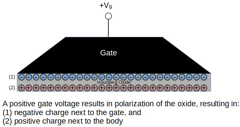
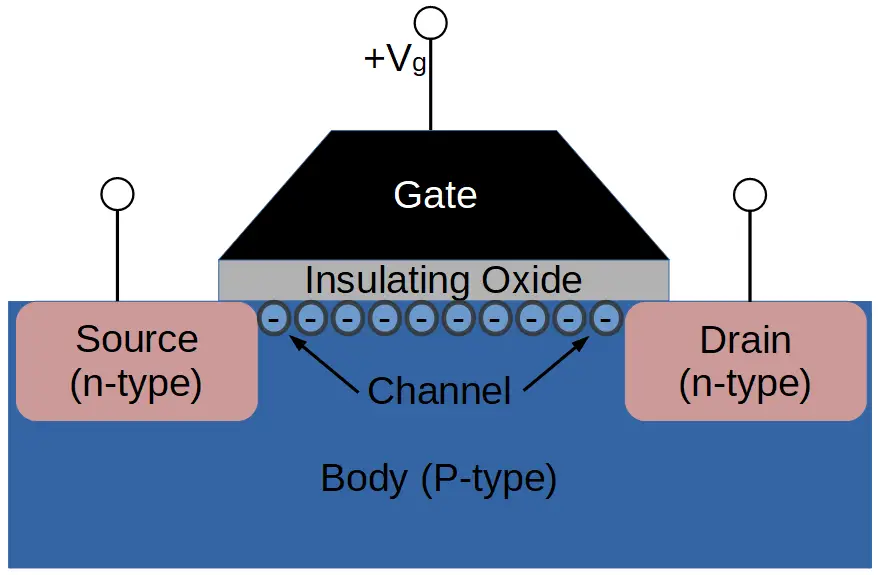
The positive charge in the oxide is located next to the body, and attracts any free negative charge in the p-type body. These negative charges form the channel between the source and drain.
The channel allows negative charge carriers (electrons) to flow from the source to the drain.
We can see that the channel is not a ‘mechanical’ region of the MOSFET, but it is critical to the transistors’ functionality. Formation of the channel is what allows current to flow when proper biasing is applied to the source and drain. The width of the channel is determined by the bias; a more positive voltage will result in a wider channel and greater current flow.
Source and Drain Bias
In order for the MOSFET to function, all three terminals need to have proper bias.
The bias of an MOSFET is similar to that of a BJT in that the P-N junction formed between the source and body must be forward bias in order to inject charge carriers into the transistor. Similarly, the P-N junction between the body and drain must be negatively biased in order to attract charge carriers into the drain.