Bipolar Junction Transistor (BJT)
Just as most diodes are essentially variations of a single P-N junction, a simple transistor can be made by using just two P-N junctions, which is known as a Bipolar Junction Transistor.
Bipolar junction transistors are a type of transistor that is made from three doped regions, in an PNP or NPN configuration, and which use both electrons and holes as charge carriers.
BJTs have three terminals, one for each doped region. The three terminals are called the emitter, base, and collector.
The main function of a BJT is that a small voltage across (or current through) the base and emitter can control a relatively large current between the emitter and collector. This is why transistors are sometimes considered synonymous with amplifiers. However it may be better to think about them as critical components within an amplifier circuit.
What Makes a Transistor Bipolar?
Bipolar junction transistors are called bipolar because they use both electrons and holes to conduct. As current passes through the transistor, both n-type and p-type materials contribute to electric current.
This is in contrast with unipolar devices like field effect transistors (FETs), which use only one type of charge carrier (either electrons or holes) and move through a channel that is either n-type or p-type.
Two Types of Bipolar Junction Transistor
Bipolar junction transistors (BJTs) can be thought of as two PN junctions that are placed back to back. Since there are two sides of a P-N junction, there are two ways that a BJT can be arranged; PNP and NPN.
PNP and NPN transistors are very similar in theory of operation and construction, but there are a few fundamental differences:
- In NPN transistors, current flows from the collector to the emitter. In PNP transistors, current flows from the emitter to the collector.
- In NPN transistors, the primary charge carriers are electrons. In PNP transistors, the primary charge carriers are holes.
PNP Transistor
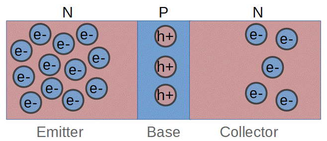
A PNP transistor can be though of as two PN junction diodes, with the p-doped sides of each facing outwards and having a shared n-type region between them.
If two P-N junction diodes were used for the construction, the n-type region of the first diode would be directly connected with the n-type region of the second diode. Therefore the action is the same as a single n-type region, which in this case would be the width of two ‘standard’ n-type regions.
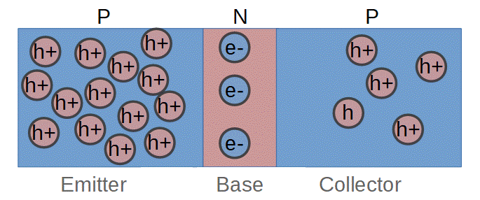
Illustration of PNP transistor. Note the narrow width of the base and high doping of the emitter region.
There are three doped regions in a PNP transistor: two p-type regions surrounding an n-type region. The p-type regions have an excess number of holes due to the addition of dopant atoms with less electrons than the substrate (usually silicon). The n-type regions have an excess number of electrons due to the addition of dopant atoms with more electrons than the substrate.
In real-life PNP diodes, the n-type base is made smaller than the n-type region in a standard P-N junction. In addition, the emitter is much more highly doped than the base and collector. The base itself is typically more highly doped than the collector. This reduces electron-hole recombination in the base, ensuring that most of the holes are swept into the collector.
How a PNP Transistor Works
In a PNP transistor, the emitter has an excess number of holes available for conduction. When a positive potential is placed across the base and emitter, these holes move toward the n-type base where a small amount of carrier (electron-hole) recombination occurs. However, unlike a traditional P-N junction, the n-type base region in the transistor is narrow and only lightly doped. As a result, most of the holes are pulled through the base region without recombining with electrons.
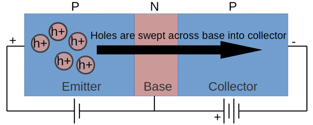
At the same time, a negative potential is placed on the p-type collector (the third region in the PNP transistor). This negative potential then pulls the positively charged free holes through the p-type collector. The holes are swept into and through the collector.
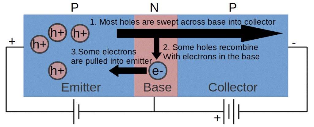
This isn’t quite the entire story, however. A small number of holes do combine with electrons in the base, and a small number of electrons are pulled from the base toward the emitter.
These carriers also contribute a small amount to conduction. This is why bipolar junction transistors are classified as using both electrons and holes for conduction. Hence the term ‘bipolar’.
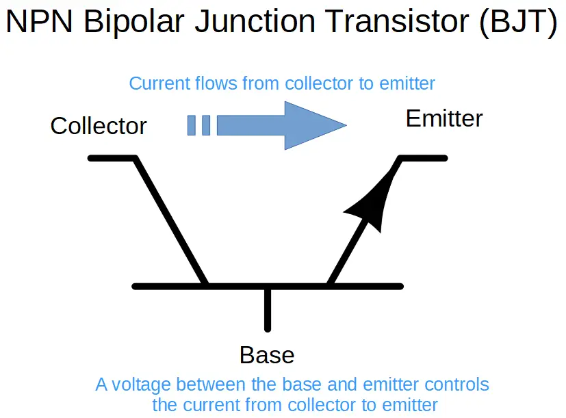
NPN Transistor
NPN transistors are very similar to PNP transistors, but operate using electrons as the primary charge carriers.
They can be modeled as two diodes with a shared/connected p-type base.
Like PNP transistors, NPN transistors are comprised of three doped regions of a semiconductor crystal. In an NPN transistor, there are two n-type semiconductors surrounding a p-type region. The n-type semiconductors have an excess number of electrons. The p-type region (in the middle) has an excess number of electron holes because it is doped with atoms that have less atoms than the substrate.
How an NPN Transistor Works
In an NPN transistor, the main charge carriers are electrons, which are supplied by the n-type emitter. The action is fundamentally the same as with the PNP transistor, but current always travels opposite the direction of electron flow. In a PNP transistor, hole flow is in line with the current, because holes are modeled as positively charged particles.
Since electrons flow from the emitter to the collector in NPN transistors, this means that current flows in the opposite direction; that is, from the collector to the emitter.
A negative potential is placed across the base and emitter. The excess free electrons in the emitter are pushed toward the base, where a small percentage recombines with a small number of holes. The doping level of the emitter is much higher than that of the base however, so there are far more free electrons than holes. Instead, the majority of the electrons are pulled through the base into the collector.
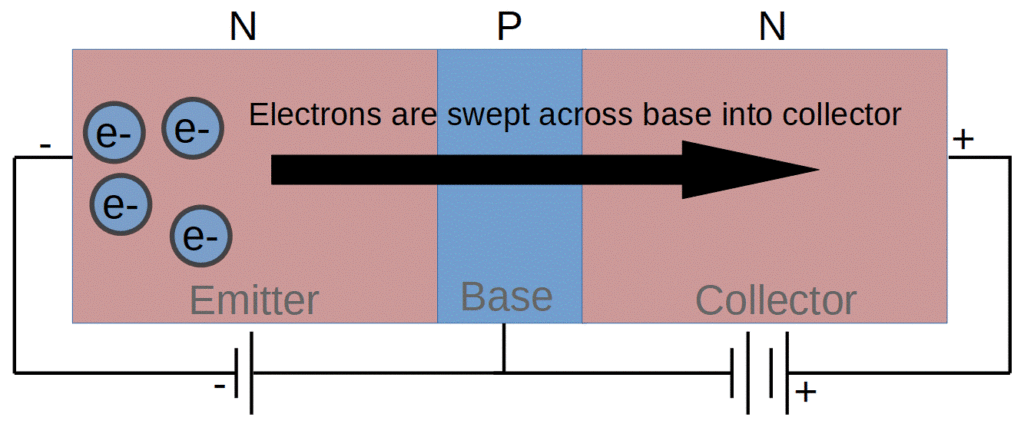
A small number of holes also makes its way from the base into the emitter, aiding in emitter-base current.
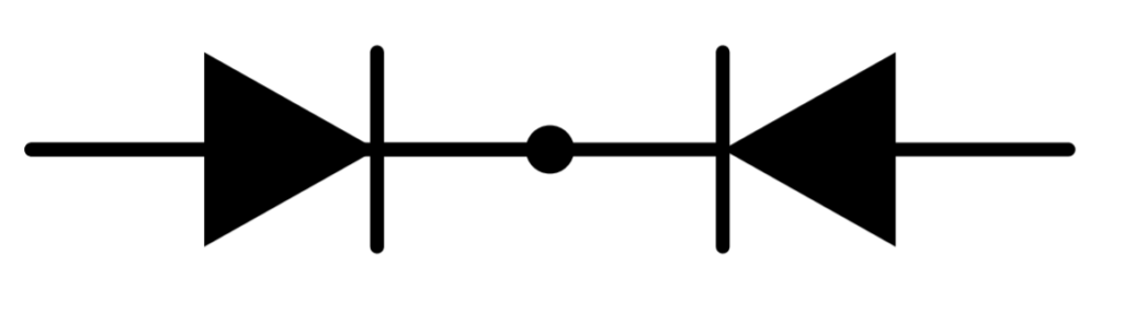
The Two Diode Model
Testing a Bipolar Junction Transistor With a Multimeter
Using the example of two diodes to model a bipolar junction transistor is useful not only for comprehension, but also for testing BJTs. A multimeter can be used to test basic functionality as long as it has an integrated diode tester.
In this case, you can simply use a multimeter to check each ‘diode’, with an additional check to ensure that the transistor does not have a short circuit.
Testing a PNP Transistor With a Multimeter
- Using the multimeter in ‘diode testing mode’, perform two tests: one from the emitter to the base, and one from the collector to the base. If the multimeter does not have a diode testing function, you can also use a resistance function.
- Check the resistance from the emitter to the collector. This resistance value should be high.
Testing an NPN Transistor With a Multimeter
- Using the multimeter in ‘diode testing mode’, perform two tests: one from the base to the emitter, and one from the base to the collector. If the multimeter does not have a diode testing function, you can also use a resistance function.
- Check the resistance from the emitter to the collector. This resistance value should be high.
The Two Diode Model Isn’t Perfect
Although the ‘two diode model’ is good starting point for understand BJTs, it does have some limitations.
In particular, the base of both PNP and NPN diodes is very different from the ‘middle region’ of the two diode model. First, the base is one single region, whereas the middle region of the two diode model is two distinct regions connected by a conductor. Second, the base is much narrower than the n-type region in a standard P-N junction diode. Third, the base is very lightly doped compared with the emitter, which is the most heavily doped region of a BJT.
These factors reduce carrier recombination in the base. They allow the BJT to function primarily via minority carrier diffusion from the base to the collector. The term ‘minority carrier’ means that the primary contributor to current is the charged particle with the opposite polarity of the free charges in the base. For instance, a PNP transistor functions by injecting holes into the base, where they are the minority carrier whereas an NPN transistor injects electrons into the base. Holes are a minority carrier when they are in an n-type material, and electrons are a minority carrier when they are in a p-type material.
Bipolar Junction Transistor Modes of Operation
There a four modes of operation for bipolar junction transistors: forward-active, saturation, reverse-active, and cut-off.
Forward-active
This is the standard mode of operation for most BJTs. The base-emitter junction is forward biased, and the base-collector junction is reverse biased. A small change in the base-emitter bias yields a large change in emitter-collector current, called gain.
Saturation
In saturation mode, both junctions are forward biased. This allows a maximum emitter-collector current, but the transistor does not function as an amplifier.
Reverse-active
If the bias of the forward-active mode is reversed (or the transistor reversed), the transistor can be made to operate ‘backwards’, with the emitter functioning as collector and vice versa. In this case, the gain is much smaller than in the forward-active configuration.
Cut-off
With both junctions reverse-biased, emitter-collector current will be very low.
Bipolar Junction Transistor Amplifiers
BJTs can be configured by placing them into an amplifier circuit in one of three different ways. These are called common base, common emitter, and common collector configurations.