The 555 timer is one of the most important and popular integrated circuits of all time. This article presents an in-depth introduction to the 555 timer circuit. We’ll learn what the 555 timer is, how it works, and why it remains incredible popular decades after its initial release.
Introduction to the 555 Timer
The 555 timer is arguable the most popular integrated circuit (IC, or chip). An integrated circuit is a collection of electronic circuits on a small, flat piece of semiconductor material. The integration of a large number of tiny components into a small chip, results in circuits that have an order of magnitude smaller, faster and less expensive than those built with discrete electronic components.
Integrated circuits contains common components like resistors, capacitors, transistors, and diodes, often in large quantities. Compared with the integrated circuits used in modern computers, the 555 timer is relatively simple. The classic 555 timer consists of a small number of common components:
- 15 resistors
- 2 diodes
- 25 transistors
But what does it actually do?
The 555 timer is an integrated circuit that produces accurate clock pulses. It is used in various timer, delay, pulse generation and oscillator applications. There are also variations having two (the 556 timer) or four (the 558 timer) timing circuits in a single package.
The 555 timer was first commercialized in 1972 by Signetics. Many companies also manufactured the original bipolar timers and similar low-power CMOS timers. In 2017, it was said that more than one billion 555 timers are produced each year according to many estimates, it is probably the most popular integrated circuit ever made. This component is still used today because of its practicality, efficiency, low cost and stability. It is often combined with other common components and analog ICs like operational amplifiers to create different circuits.
History of the 555 Timer
In 1968, Hans Camenzind was hired by Signetics to develop a Phase Locked Loop (PLL) integrated circuit. He designed an oscillator for PLLs so that the frequency does not depend on the supply voltage or temperature. Afterwards, Signetics froze development on the PLL due to the recession in 1970.
Camenzind proposed the development of a universal oscillator-based circuit for PLLs and asked to develop it on his own, borrowing equipment from Signetics. The marketing manager of Signetics approved the idea and the first design of the 555 IC was updated in the summer of 1971.
After the design was updated and considered without errors, Signetics proceeded to design the layout. Later, Camenzind had the idea of using a direct resistor instead of a constant current source. The change reduced the required 9 pins to 8 so that the IC could be inserted into an 8-pin package instead of a 14-pin package. The 555 timer was manufactured by 12 companies in 1972 and has become a best-selling product.
Several sources report that the name 555 comes from the three 5-kilohm resistors inside the chip. However, in a recorded interview with an online curator of the transistor museum, Hans Camenzind said “It was just arbitrarily chosen. It was the then-marketing-manager of Signetics; Art Fury; who thought the chip would sell big who chose the name ‘555’.”
555 Timer Packages and pinout
555 Timer Packages
DIP-8: Dual In-line Package is one of the oldest IC packages still in use today and many ICs come in this package. It is known by its rectangular shape and has wires running on both sides along its length, forming two sets of in-line pins. The DIP-8 version of the 555 timer is an 8-pin component and has the following dimensions: 9.81 mm × 6.35 mm.
SOP-8: Small Outline Package is a type of surface mount IC package. They are very low-profile (about 1mm) and have tight lead spacing. The SOP-8 version of the 555 timer is an 8-pin component and has the following dimensions: 6.20 mm × 5.30 mm.
555 Timer Pinout
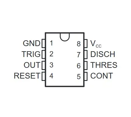
GND – 1: Ground, this pin is the reference voltage to ground (zero volts).
TRIG – 2: Trigger, when the voltage on this pin drops below 1/3 VCC – except when the control is driven by an external signal – the output goes high and a synchronization interval begins. As long as this pin continues to be held at low voltage, the OUTPUT will remain high.
OUT – 3: Output, this pin is a Push-Pull output that is driven to a low state (GND) or a high state. For bipolar timers, this pin can drive up to 200 mA, but CMOS timers are capable of driving less depending on the chip.
RESET – 4: a synchronization interval can be reset by driving this pin to GND, but the synchronization will not restart until this pin exceeds approximately 0.7 volts. If this pin is not used, it should be connected to VCC to prevent electrical noise from accidentally causing a reset.
CONT – 5: Control, this pin provides access to the internal voltage divider (2 ⁄ 3 VCC by default). By applying a voltage to this pin, the timing characteristics can be changed. In astable mode, this pin can be used to modulate the OUTPUT pin in frequency. If this pin is not used, it must be connected to a 10nF decoupling capacitor then to GND to ensure that electrical noise does not affect the internal voltage divider.
THRES – 6: Threshold, when the voltage on this pin is higher than the voltage at the CONTROL pin (THRES > CONT) which indicates the end of timing input, it sets OUTPUT low and DISCH low.
DISCH – 7: Discharge, for bipolar timers, this pin is an Open Collector (OC) output, whereas CMOS timers are Open Drain (OD). This pin indicates the start of timing. When TRIG < 1/2 CONT it sets the output high and DISCH open. In bistable mode this pin is unused, so it can be used as an alternative output.
VCC – 8: Positive power supply, for bipolar timers, the voltage range is generally 4.5V to 16V, some are specified for a maximum of 18 volts, although most can operate as low as 3V. For CMOS timers, the voltage range is generally 2V to 15V, some are specified up to 18 volts, and some are specified as low as 1V.
Decoupling capacitors are usually applied between this pin and GND as a good practice.
How the 555 timer works
555 Timer Circuit diagram
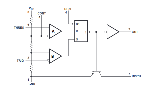
Inside the 555, is the equivalent of 20 transistors, 15 resistors, and 2 diodes, depending on the manufacturer.
Inside, there are three identical resistors which divide the supply voltage into 3 equal parts. If the circuit is powered with a 9V battery then, each of the resistors will cause a voltage drop of 3V. The purpose of dividing the supply voltage into 3 parts is to provide the comparators A and B with reference voltages which will be equal to 1/3 and 2/3 of the supply voltage.
Each of the 2 comparators has one pin connected to a reference point, either 1/3 or 2/3 of the supply voltage. The other pin of each comparator, i.e. connection pins 2 and 6, are linked to their corresponding output pins.
The comparator B acts only if the voltage on TRIG pin falls below the threshold of 1/3 of the supply voltage. When this happens, it sends a pulse to the flip-flop so that it does a Reset (Low state) on its output. And the transistor connected to the output of the flip-flop will then go into blocking mode, stopping the flow of current.
The comparator A acts only if the voltage on THRES pin exceeds the threshold of 2/3 of the supply voltage. When this happens, it sends a pulse to the flip-flop so that it makes a Set (High state) on its output. And the transistor connected to the output of the flip-flop will then go into saturated mode, allowing the current to flow.
555 Timer Modes
The 555 timer has the following operating modes: astable, monostable, and bistable.
Astable mode
The 555 timer can operate as an electronic oscillator. Uses include LED and lamp flashers, pulse generation, logic clocks, tone generation, safety alarms, pulse position modulation, etc.
In astable mode, the 555 IC can be used as a simple ADC, converting an analog value into a pulse length (for example, selecting a thermistor as a timing resistor allows the 555 to be used in a temperature sensor and the period of the output pulse is determined by the temperature). The use of a microprocessor circuit can then convert the pulse period to temperature, linearize it and even provide calibration capabilities.
Monostable Mode
A monostable circuit means that the output of the circuit remains at a logic level when nothing happens on its control input. But when a pulse is applied to its control input, the output goes to the opposite logic state, for a given time.
In this mode, the 555 functions as a “one-shot” pulse generator. The 555 timer generates a single pulse when the timer receives a signal from the trigger input pin. The duration of the pulse depends on the values of the resistors and capacitors around the circuit. If a trigger pulse is applied to the input via a push button, then the capacitor is charged and the timer develops a high pulse, then it remains high until the capacitor discharges completely. If it is necessary to increase the time delay, a higher resistor and capacitor values are required.
Applications of the 555 IC in this mode include timers, missing pulse detection, no-bounce switches, touch switches, frequency divider, capacitance measurement, pulse width modulation (PWM), etc.
Bistable Mode
The 555 IC functions as an SR flip-flop. And applications in this mode include locked switch debouncing circuits.
In this mode, the timer circuit 555 produces two stable state signals, a high and a low states. The output of the high and low state signals is controlled by reset and triggering the input pins, not by charging and discharging the capacitors. If a logic low signal is given to the trigger pin, then the output of the circuit goes high. If the logic low signal is given to the reset pin, then the output of the circuit goes low.
555 Timer Output specifications
The output stage consists of several transistors allowing the 555 timer to supply or absorb up to 200 milliamps on its output.
For more current, it is necessary to use a transistor on the output, like the 2N2222, which is capable of handling up to 800 milliamps.
General Specifications
The 555 IC was the first timer circuit or time base. It is suitable for DIYs or professionals in a stable, user-friendly way for monostable and astable applications.
The main specifications of this component are:
- Maximum pulse speed less than 2ms
- Time base can be from a few microseconds to hours
- Works in bistable, monostable or astable mode
| Specification | Value | Unit |
| Supply voltage (VCC) | 4.5 – 16 | V |
| Supply current (VCC = +5V) | 3 – 6 | mA |
| Supply current (VCC = +15V) | 10 – 15 | mA |
| Max. output current | 200 | mA |
| Max. power dissipation | 600 | mW |
| Operating temperature | 0 – 70 | °C |
| Max. frequency | 2 | MHz |
* The above specifications apply to the bipolar NE555 timer. Other versions of the 555 timer may have different specifications.
555 Timer Applications
In concrete terms, this IC is an “electronic timer”. It is therefore possible to make a timer (time function, delay), an alarm siren (oscillator function, astable), a threshold detector (bistable), or a calibrated pulse generator (monostable).
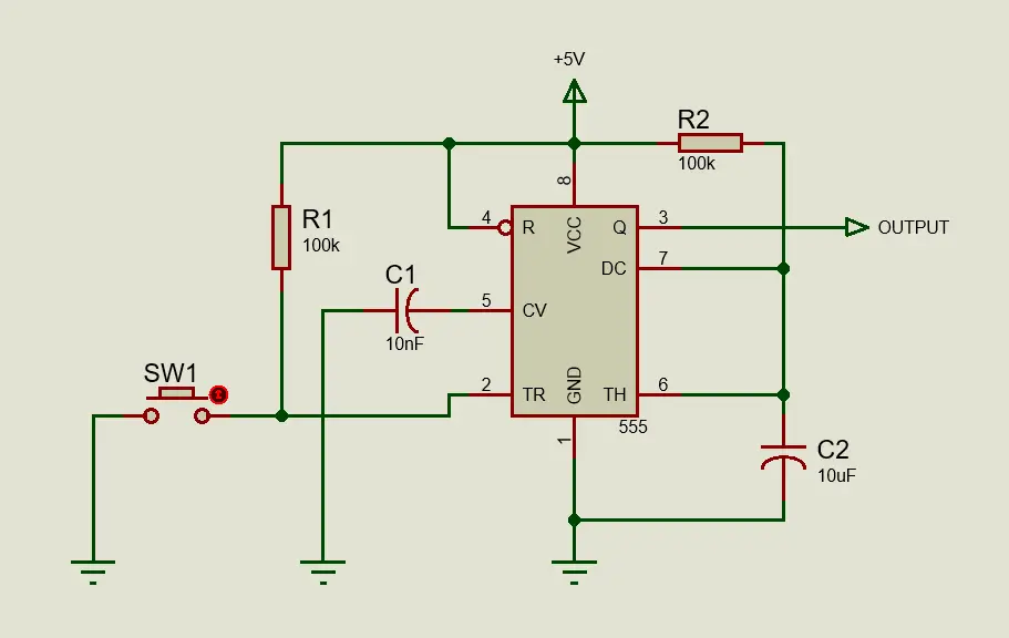
Switch Debouncing Circuit
Many physical switches can bounce for hundreds of microseconds after being pressed, while most logical devices respond in only a few nanoseconds. This can lead to false triggers and erroneous outputs. By adding an appropriate debouncing circuit between the switch (Button, Switch…) and the logical device, these bounces can be reduced or even eliminated.
In this circuit, when pushbutton switch SW1 is closed, the output toggles from LOW to HIGH. Later when input switch SW1 is opened the output of the 555 IC remains HIGH for a delay period. After the delay period – which is about 1 second for this circuit – the output toggles from HIGH to LOW.
The delay period can be adjusted for this switch debouncing circuit. One method of adjusting the time delay is to change the capacitance value of C2. Decreasing the value of C2 will decrease the delay time at the output of the 555 IC. Increasing the capacitance value of C2 will increase the delay time.
Timed relay
This is a simple solution for keeping a relay energized after pressing a pushbutton for a period ranging from thirty seconds to one minute.
This project is very useful in applications like: switching on the lighting of a staircase or a corridor for a certain period of time. Or to keep the siren of an anti-theft system on. Or to control an extractor hood in a kitchen or a bathroom ventilation.
This circuit uses a NE555 timer to drive the base of an NPN transistor which can then drive high load components. To vary the excitation time (the time the relay is powered) of the relay simply turn the variable resistor R3 connected between R2 and pins 6 and 7 of the 555 timer. And to increase the maximum duration, you must increase the capacity of the electrolytic capacitor C1.
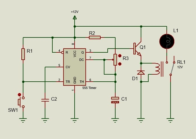
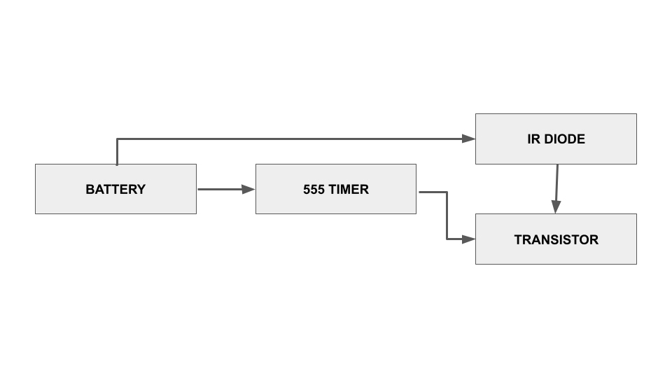
TV remote control jammer
This project is used to block emerging signals from the TV remote control by generating pulses from the infrared sensor connected to an NE555 IC. This project is designed with a 555 timer operating in astable mode that generates high power pulses that are transmitted to the IR sensor. The IR sensor produces IR beams in the 38 KHz range, these beams prevent the IR beams from leaving the TV remote control.
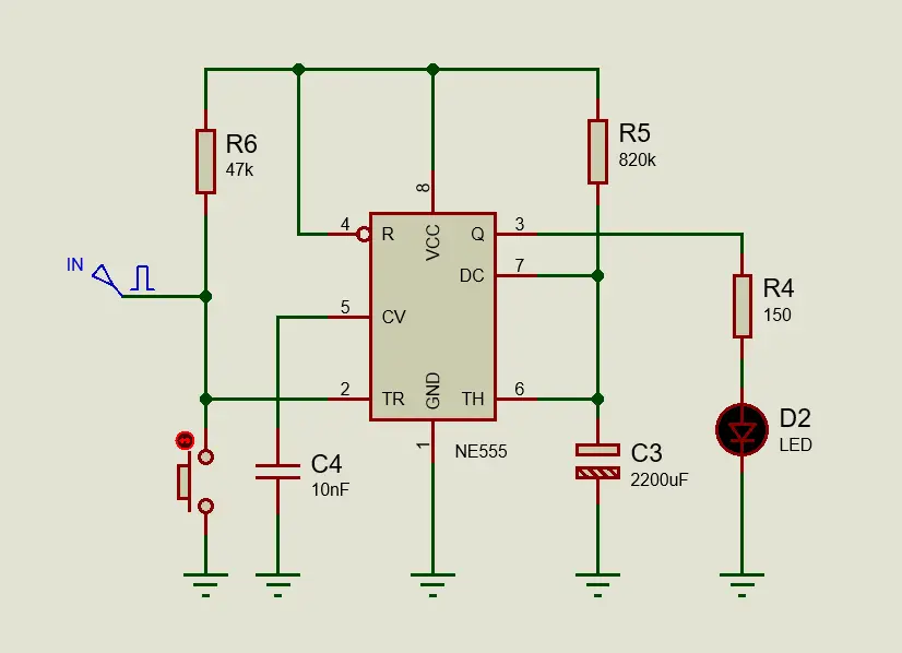
Long duration timer
If you want to have a long duration timer while keeping a reasonable value of capacitors and resistors in your circuit, it is appropriate to think about a circuit using an integrated circuit style timer like the NE555 IC.
This NE555 based circuit allows to reach a duration of about half an hour with a 2200uF capacitor and an 820kOhm resistor, provided that the capacitor is of good quality and has a low leakage current (the highest possible parasitic parallel resistance). If the capacitor is not of good quality or is too old, its leakage current will prevent it from charging at two-thirds of the supply voltage (2/3 VCC) (the NE555’s “upper” switching threshold) and the output will always remain on.
Triggering the circuit is done by bringing pin 2 of the NE555 to ground. This is what the pushbutton in the circuit does when pressed. By replacing the pushbutton with a capacitor, you get a timer that is triggered when the power is turned on, and stops by itself when the timer time is reached.
Alternatives to the 555 Timer
7555 Timer
The 7555 circuit is a modified 555 timer. This IC does not use bipolar transistors but field effect transistors (FET). Therefore, in addition to consuming very little current, its operating voltage is extended (between 2V and 18V).
This model in particular is suitable for precision timers supplied with very low voltage. Other models have different characteristics. Some can oscillate up to several MHz, others can operate at very low voltages (from 1V for some models). However, these circuits are much more expensive than the standard 555 IC and are produced on a smaller scale. This is why they are not very accessible to the general public.
556 timer
The 556 timer is the dual version of the 555 timer. It includes two complete 555 timers in a 14-pin package, and only the two power pins are shared between the two timers. The bipolar version is available as NE556, and the CMOS versions were available as ICM7556 for Intersil and TLC556 and TLC552 for Texas Instruments.
It works the same way and the pin names are identical. The only notable difference is that its outputs (pins 5 and 9) can drain less current, 150 mA only, in some manufacturer’s references.