What is Semiconductor Physics?
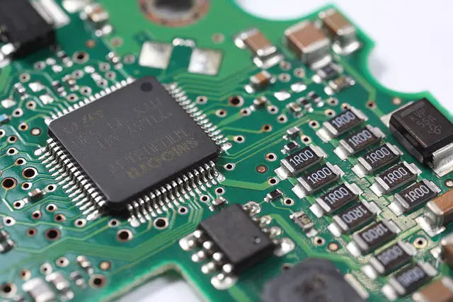
Semiconductors are used to produce much of the incredible technology that we see around us in the world today. The most common semiconductor devices include many different types of diodes, transistors, and sensors as well as photovoltaics (solar power cells).
Semiconductor physics is the field of study of how semiconductor devices work at a fundamental level. While experimentation and an application-based understand can teach us how a given diode or transistor function in practice (commonly described using an I-V curve), semiconductor physics can tell us why they function the way that they do.
This allows us to understand them much more deeply and to learn how the structure of the semiconductor device leads to its’ behavior. In turn, this leads to the development of new devices or the improvement of existing ones.
Why Learn Semiconductor Physics?
Semiconductors are some of the most important creations of humankind. They provide the building blocks of most of our electronics and virtually all of our computational systems. This includes our desktops, laptops, cell phones, servers, and satellite communications systems. Our modern world would not be possible without them.
This is poetically described by the term ‘silicon age’, which signifies that like the stone, bronze, and iron ages, the course of humanity is often powerfully interwoven with the primary materials that we use to shape the world around us. Silicon, the most abundant element in the earth’s crust, is a semiconductor.
In order to understand how we can take silicon and use it to change our societies and our relationships between each other and technology, we need to learn how silicon actually works. This requires some knowledge of semiconductor physics.
Transistors Keep Getting Smaller
Semiconductor physics isn’t just about understanding devices as they currently are; it’s also about learning the fundamentals so that we can tackle the problems that will face the semiconductor industry in the future.
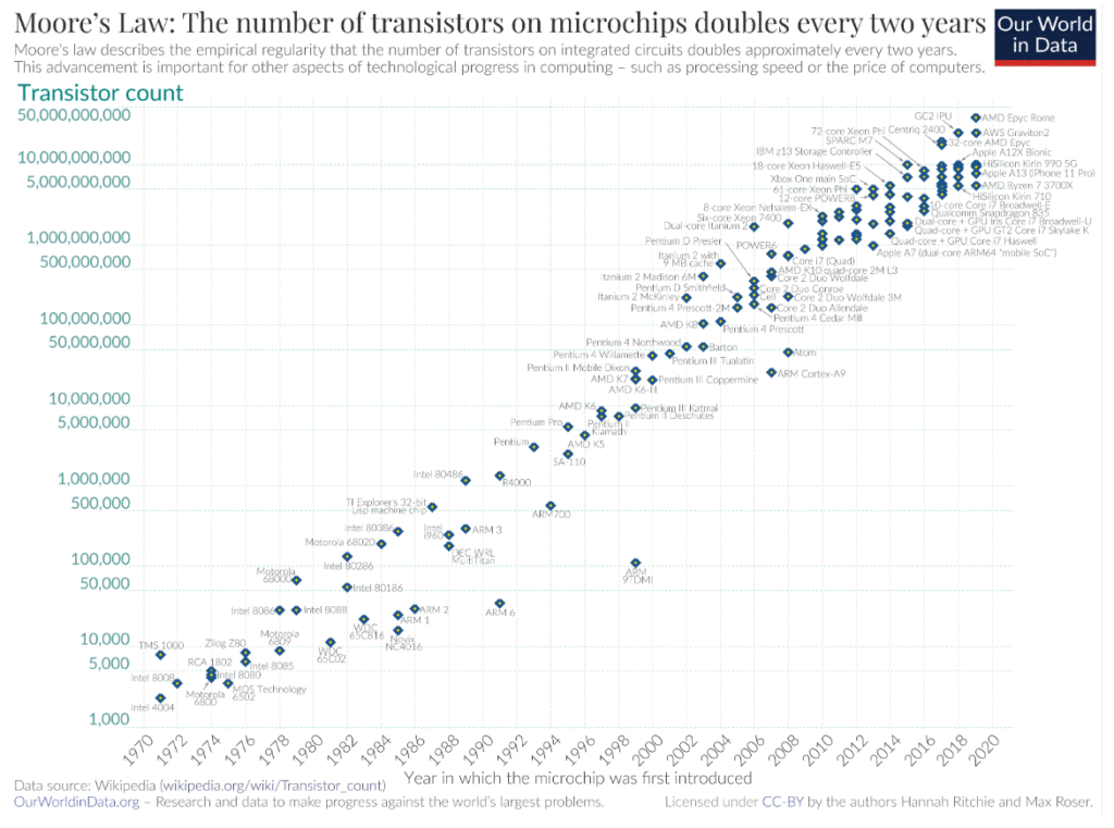
The transistor is one of the most important devices in electronics, and has been shrinking in size since 1947. Every reduction in size leads to greater performance and reduced cost.
The problem is that we can’t continue to reduce the size of the transistor forever without influencing the fundamental properties of the device. Put simply, electrons act much differently when they are travelling through a bulk material than they do when they are confined in an atomic-scale system.
This is because at near-atomic levels, quantum mechanical effects begin to dominate the functionality of the device. At that point, we can no longer rely on the models that have historically been so successful in predicting the behavior of the device.
We therefore need new models that are based on quantum mechanics.
This is not specific to semiconductors. In physics, the models that govern classical mechanics (based on Newton’s laws, Hamiltonians, Lagrangians, special and general relativity) must give way to quantum mechanics when dealing with objects of extremely small sizes.
Semiconductor physics is the logical extension of this, specifically applied to help us understand how devices will behave as they become smaller and smaller.
The Transistor as a Switch
The standard metal-oxide-semiconductor transistor is most commonly used as a switching device that provides the underlying functionality of manipulating bits in a computer. When the transistor is switched ‘on’, this state is interpreted as a logical ‘1’. When it is ‘off’, it is a logic state of ‘0’. The binary zeroes and ones as given by transistor state are therefore the backbone of digital computers.
Transistors as switches are also combined with each other to produce logic gates such as AND, OR, NOT, and XOR. This is why when we think of modern semiconductor devices, we tend to think of transistors. Other semiconductor devices like diodes are given a bit of a backseat due to the criticality of transistors in general (i.e. why Moore’s Law is a reflection of transistor size rather than diode size).
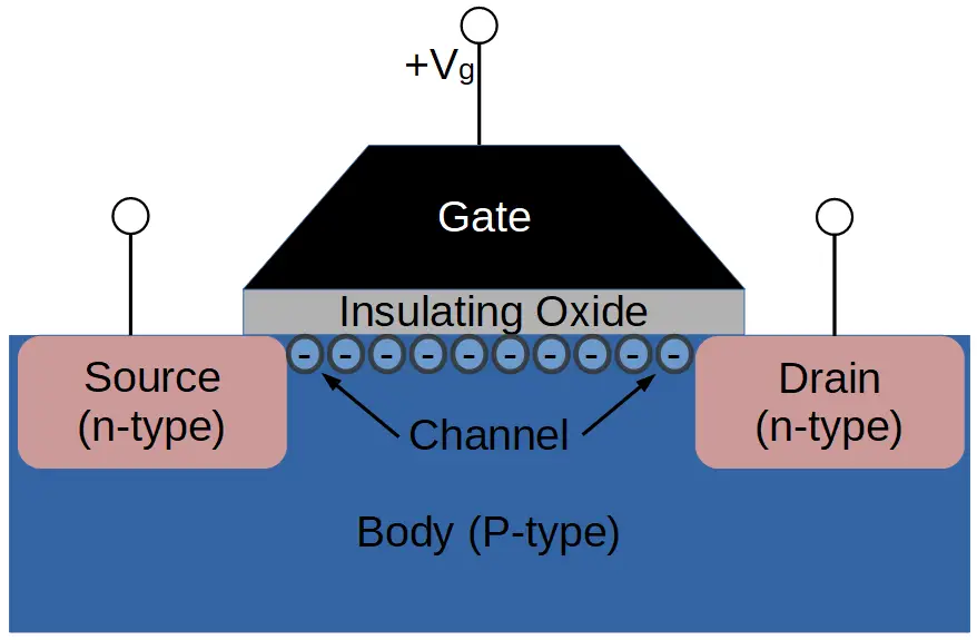
MOSFETs (metal oxide semiconductor field effect transistor) are the most common type of transistor used in computers. In a MOSFET, current travels from the source to the drain through a region called the channel and is controlled by a potential difference (voltage) across the gate. The gate is electrically insulated from the source and drain so that current does not actually flow through the gate. Rather, the amount of voltage applied across the gate controls current between the source and drain.
Over the years, the size of the source, gate, and drain has decreased drastically. The original transistor created by William Shockley’s team at Bell Labs was quite large. Cutting-edge transistors today have features that approach the atomic scale.
The shrinking of transistors has been in part predicted, and in part guided by Moore’s Law.
The Single Electron Transistor
As the size of the transistor is decreased, we eventually reach a point where the channel length (between the source and drain) is only a few atoms long. It’s size approaches that of a quantum dot.
At this point, only a few, and in the extreme case, only one electron may pass through the channel at a time. This means that we need to gain an understanding of how the electron occupies the electronic states available to it due to this quantum confinement.
Our classical models for understanding the behavior of the electron no longer work because the electron begins to act increasingly like a wave. We enter a world of discrete energy levels and effects such as quantum tunneling.
In order to understand and work with nanotechnology, we have to understand the principles of nanoscience.
Once we understand the basic behavior of electrons in atomic-scale devices, we can then model and develop devices that rely on those behaviors.
Nanoscience and Nanotechnology
Semiconductor device physics is deeply intertwined with nanoscience and nanotechnology.
Nanotechnology is all about the fabrication of nanostructures – materials whose dimensions are on the nanometer scale. If we have nanostructures whose lengths range from 1 to 100 nm, and the structures are made from silicon, then the structure itself is about 4 to 400 atoms thick.
The electronic, optical, and thermal properties of materials this small are markedly different from those of bulk solids.
These new properties can lead to the development of new devices that rely on the quantum mechanic based functionality as well as better performance.
In this course, we will develop the basic nanoscience that underlies modern semiconductor devices.