Moore’s Law
For decades, Moore’s Law has been a topic of frequent discussion in the world of IT and semiconductors.
Moore’s Law is an observation-based prediction that the number of transistors inside integrated circuits (ICs) will double approximately every two years.
In recent years, this dialogue has become more of a debate, with some observers claiming Moore’s Law to no longer be true, while manufacturers fight back with new technologies in the development pipeline.
In this article, we’ll explore Moore’s Law in detail. We’ll look at the history of computers and semiconductors relative to Moore’s Law and we’ll discuss what we can expect in 2021 and beyond.
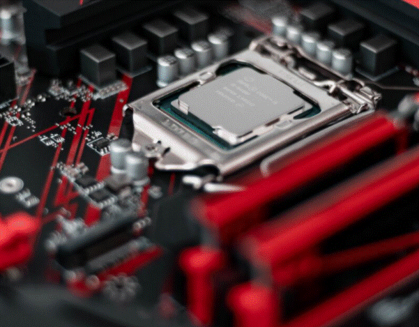
Central processing units are the most important integrated circuits in computers. Modern CPUs contain billions of transistors.
What is Moore’s Law?
Moore’s Law is one of the most important and powerful ideas in electronics.
Semiconductor companies have used Moore’s Law as a landmark to set goals and determine if they are making progress at the right pace. However, it is often misunderstood or misinterpreted.
The Moore’s Law plot on the right shows how transistor count has increased since 1970. Every generation of new integrated circuits (computer chips) contains more transistors, which increases processing power and memory while making them faster and more efficient.
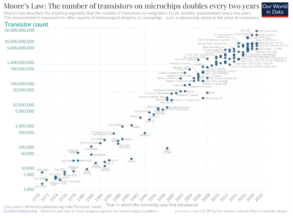
Moore’s Law plot. Image courtesy of Hannah Ritchie and Max Roser.
In the early 1970s, integrated circuits contained several thousand transistors. By 2020, this number had increased to almost 50 billion.
Why is Moore’s Law so Important?
Transistor Based Technology
Moore’s Law is a prediction of the number of transistors in integrated circuits. In order to understand Moore’s Law, we need to understand transistors and why they are so important.
Transistors are electronic devices that can be manufactured to really small sizes. Some transistors are just a few atoms long. Most transistors in computers are a type of Field Effect Transistor, or FET.
Simple FETs have a drain, gate, and source. Current flows from the drain to the source, but it is controlled by the gate. You can think of the gate as a valve that determines the amount of current that makes it to the source. Current through the transistor determines a binary value of 0 or 1, the language of computers.
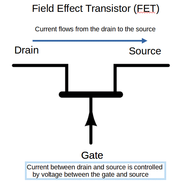
When the gate allows current to flow, it switches the transistor ‘on’. An ‘on’ signal is interpreted as a ‘1’, and an ‘off’ signal is a ‘0’ in the binary language of computers. More transistors means more 1’s and 0’s; every transistor contributes to a computer’s performance.
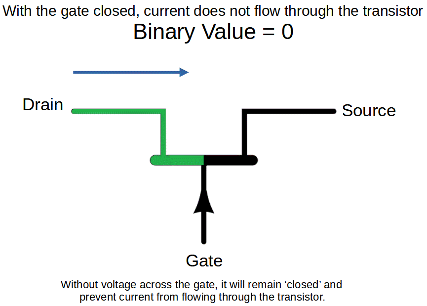
Without a voltage across the gate, the transistor is ‘off’. Current will not not flow through the transistor.
This corresponds to a binary value of 0. This is also expressed as a logic value of ‘false’.
When a voltage signal is detected, the gate allows current to flow and the transistor is switched ‘on’. Computers interpret this as a binary value of 1. This is also expressed as a logic value of ‘true’.
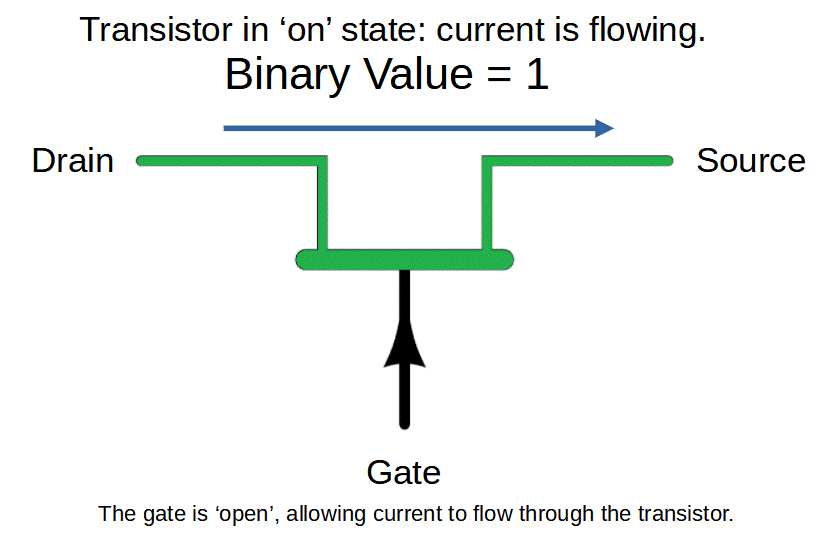
More transistors equals more 0’s and 1’s with which the circuit can deal. Therefore, more transistors means more powerful computer processors and more storage in memory chips.
This is the main reason that Moore’s Law is so important. The exponential growth of the number of transistors in computer chips predicted by Moore’s Law also corresponds with exponentially more powerful computers.
Dawn of The Information Age
In order to understand the full impact of Moore’s Law on human civilization, we have to analyze the potential power inherent in computers and the transfer of information.

The Z3 was the world’s first programmable digital computer, produced in 1935.
The 20th century saw a rapid transformation from traditional industry based on the Industrial Revolution into a computer based economy. The historical period marked by the increasing presence of computers in our daily lives, which began in the 1950s, has come to be known as the Information Age. The Information Age has deeply affected our economies, cultures, and even the way we think. In large part, this has to do with increased information transfer between people across the planet.
This isn’t the first time information-based technology has altered the course of human history (and it probably won’t be the last).
Around 1440 CE, Gutenberg’s printing press resulted in a revolution in information transfer, enabling communication and sparking the ever-quickening process of scientific and technological development.
The power of the new press was that it sped and enhanced communication between people. In one century, unparalleled advances in every branch of science led to the beginning of the scientific revolution. Literacy increased dramatically, shifting the balance of power from the royal and elite to the common people in what is now called the democratization of knowledge. These developments led to the Enlightenment period and, in an interesting parallel to modern times, occasional widespread misinformation due to the spread of ‘fake news’.
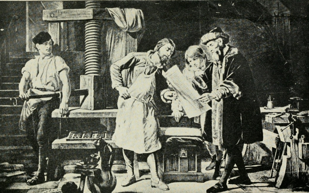
A recreation of Johannes Gutenberg and his printing press. Less than 25 million books were printed during the entire 15th century. By the 18th century, book production skyrocketed to nearly 1 billion.
All of these developments occurred due to a single new technology that enhanced information transfer.
Surprisingly, the printing press remained relatively unchanged for several centuries. A single, relatively stagnant new technology resulted in centuries of unprecedented development, because it enhanced communication between people.
What would happen if an information-based technology was created that would feed into its’ own development via improved computation and technical capabilities?
The answer is an exponential increase in technological achievement over time. This is Moore’s Law.
From Early Computers to Moore’s Law
The story of Moore’s Law is one of past, present, and future. In order to chart the progress in computing described by Moore’s Law, we need to start at the beginning.
Early 20th Century: Gears, Relays, and Vacuum Tubes
The first computers were mechanical, employing gearing systems to perform numerical operations. These early computers were basically mechanized versions of the abacus. They were mostly focused on making it easier to count things.
Over time, mechanical computers became more sophisticated and able to perform functions beyond counting. The Babbage difference engine (shown on the right), designed in the 1820’s, could perform complex polynomial calculations like logarithms and trigonometric functions.
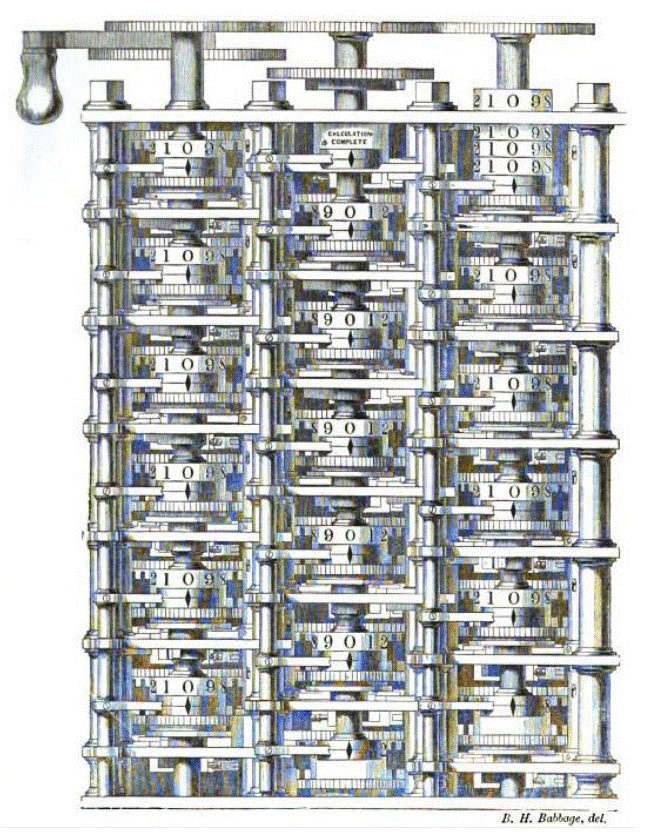
The Babbage Difference engine was a sophisticated mechanical computer.
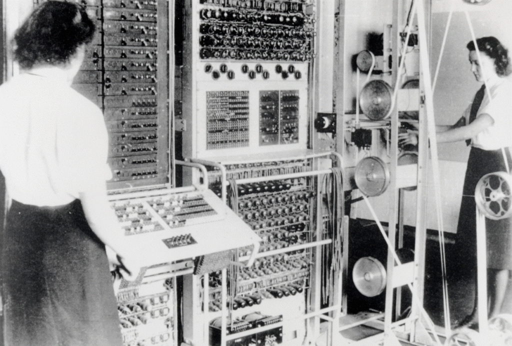
Colossus was a vacuum tube based computer used to code-break German ciphers during WWII.
The 19th and early 20th centuries saw progress of research in vacuum tubes, whose amplification properties were developed with the first triodes. Like transistors, they use a switching action to generate a binary signal that allowed for logic and computation. However, triodes were fragile devices that consumed a lot of power. They were also large and difficult to scale in size. A more powerful computer required more tubes, more space for the tubes, and more maintenance of the system as a whole.
Researchers were looking for a superior technology to replace triodes and developed theoretical models for transistors in the 1920’s and 30’s. Semiconductors at the time were not of high enough quality to create these devices. The first transistor would have to wait until high quality silicon or galena based semiconductors could be produced.
Or so it was thought.
1940’s: Germanium Sparks the Semiconductor Industry
Shortly after WWII ended, Bell Labs formed a solid state physics group, which was led by William Shockley and included physicists John Bardeen and Walter Brattain. One of their primary goals was to produce the transistor that had been theorized but never successfully built.
In December 1947, Bardeen and Brattain developed the first transistor using a germanium substrate from Purdue. Known as the point contact transistor, Bardeen, Brattain, and Shockley were awarded the Nobel Prize in Physics for its creation in 1956. This would spark increasing R & D into semiconductors and various types of transistors.
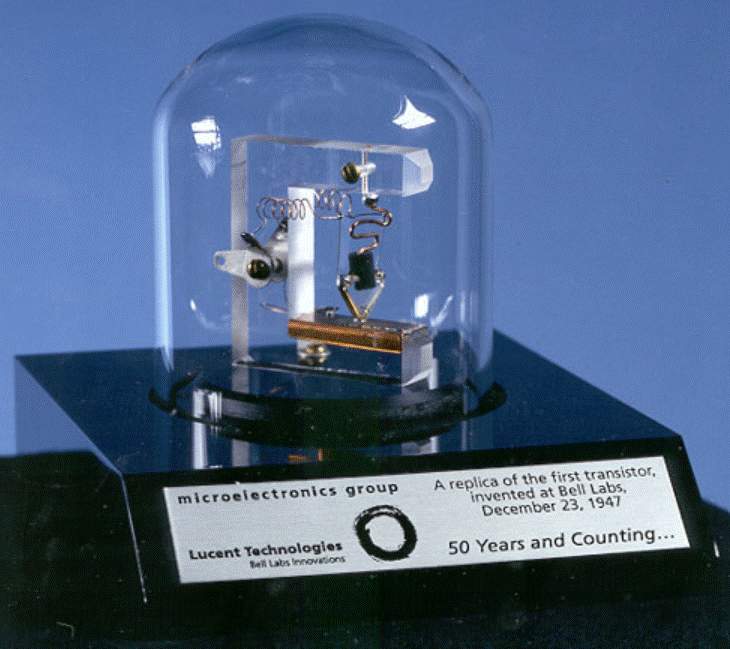
A replica of the first transistor.
Late 1950s: Silicon Becomes Reigning Champion
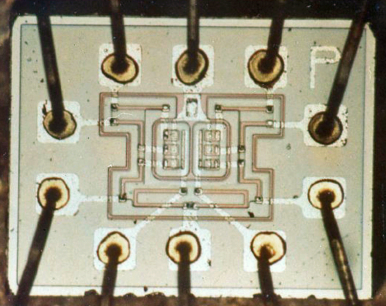
An early integrated circuit, used in the Apollo spacecraft.
All of this research into semiconductors resulted in incredible developments within a few years. Semiconductors presented not only the opportunity for new types of devices, but new methods of circuit construction as well. Integrated circuits contain an entire circuit mounted onto a single semiconductor substrate. They are stand alone circuits that can then be used reliably in more complex systems. The first integrated circuit was produced in 1958.
Then another revolutionary new semiconductor technology was developed. In 1859, Bell Labs engineers Mohamed Atalla and Bell Labs engineer Dawon Kahng developed the first silicon-based transistor. It was known as a metal oxide semiconductor field effect transistor, or MOSFET.
MOSFETs offered several advantages over the existing germanium transistors. First, silicon is incredibly abundant and therefore cheaper than germanium. Second (and perhaps more significantly), MOSFETs could be scaled to smaller size by using newly developed techniques of photolithography. It was the first transistor that could be made in sizes limited by manufacturing ability, and remains the most popular transistor to this day.
An estimated 13 sextillion (13 x 1021) MOSFETs had been produced by 2020.
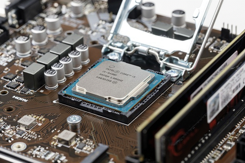
Modern CPUs contain billions of MOSFET transistors.
Due to its’ ability to be produced in smaller and smaller sizes, engineers realized that they could produce increasingly powerful chips by using more MOSFETs. By making them smaller, they could pack more chips into the same volume.
Computer technology based on MOSFETs used a fabrication technology called complementary metal oxide semiconductors (CMOS). The CMOS process enabled scaling transistors to small enough sizes that millions could now be located on a single small chip. Powerful computers that were relatively small could now be created.
1965: Gordon Moore Makes His Famous Prediction
By the early 1960’s, it became apparent that the number of transistors in integrated circuits was increasing at an exponential pace. This process of the ever-increasing number of components was described mathematically by Gordon Moore, the director of R & D at Fairchild Semiconductor.
In 1965, Moore predicted that the number of components, primarily MOSFETs, in integrated circuits would double every year for the next ten years. In 1975, he revised his estimate to a doubling of components every year for five more years and then a doubling of components every two years thereafter. His prediction has come to be known as Moore’s Law.
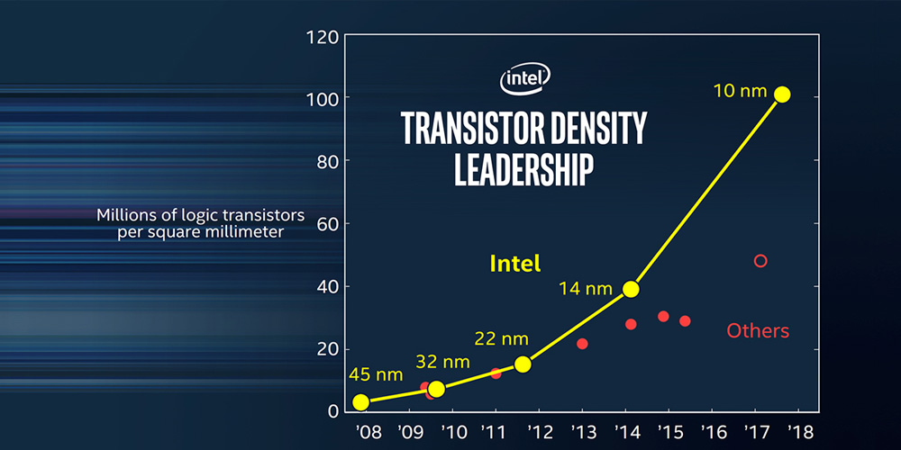
Incredibly, industry progress has closely tracked Moore’s Law since the original prediction. The plot on the right shows data from Intel, indicating that transistor density has continued to increase over the last decade.
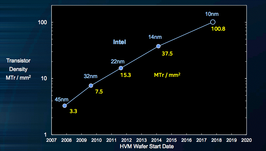
Transistor density increases since 2008. Image courtesy of Intel.
In part, this trend is due to Moore’s Law itself. Since it’s initial prediction, Moore’s Law has functioned as a goal-setting tool and self-fulfilling prophecy for the semiconductor industry. Manufacturers have set targets as close to Moore’s Law as possible, and have used those goals to drive incredible manufacturing achievements.
How Has Moore’s Law Been Achieved?
There are several primary methods by which the semiconductor industry has managed to keep a close pace with Moore’s Law.
Decreasing the Size of Transistors
The first is decreasing the size of transistors. This allows more transistors to be packed into the same volume. Transistor size decreases have been enabled by significant advances in transistor fabrication and design. Decreasing transistor size was a primary method of development for decades, but has become less important over time.
Improved Fabrication Technologies
Semiconductor fabrication technologies have been developed significantly over time, resulting in improvements to virtually every point in the process. From cleaning and etching, to the chemical photoresist and lasers used, improvements in fabrication have enabled both smaller transistors as well as improved interconnects, allowing for smaller spacing between transistors.
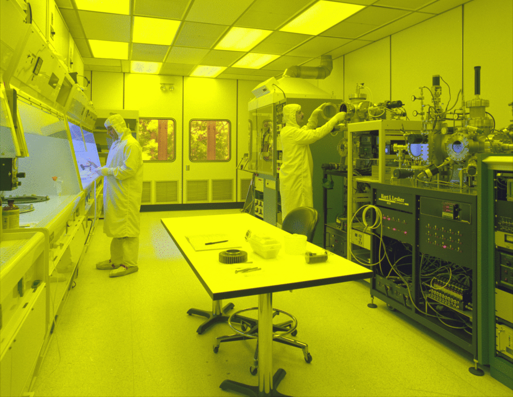
Advances in fabrication technologies have enabled Moore’s Law.
Improved Transistor Design
At nanoscale dimensions, transistors tend to experience current leakage through the gate, which became a limiting factor depending on transistor design. Developers created new transistor designs such as fin field effect transistors (FinFETs) and gate all around field effect transistors (GAAFETs). These designs significantly reduce leakage, enabling incredibly small transistors to be produced. GAAFETs have been produced as small as 3 nanometers.
What Moore’s Law Means for Computers
Better Processors
In computers, the processor is the heart of all internal operations. Processors take information in the form of binary code and perform operations on that code. Most modern processors are called microprocessors, which are MOSFET based integrated circuits.
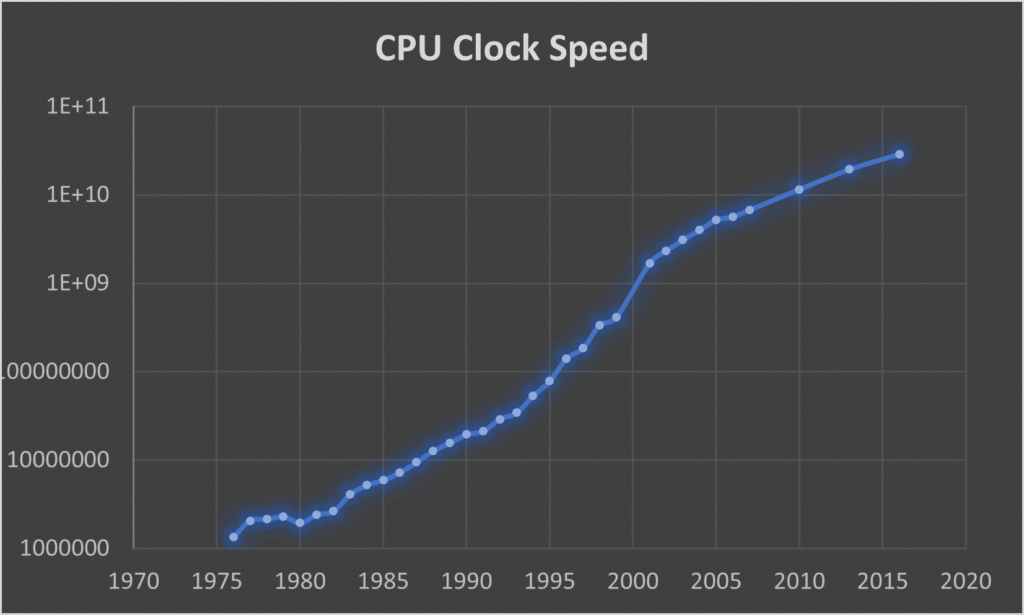
Clock Speed Data from National Bureau of Economic Research and ITRS
Processors are typically classified by their operating frequency (known as clock speed). As the number of transistors has increased over time, processors have become increasingly fast.
As predicted by Moore’s Law, the operational frequency should increase by about 40% every two years.
There are actually two primary reasons for this.
First, more transistors mean more actionable components that are available to help with computations.
Second, smaller transistors that are packed more tightly have less distance between each other, and therefore less lag time for signals to be processed.
More Memory (RAM)
Most types of computer memory are based on MOSFETs.
MOSFETs are used to store information in computer memory. More MOSFETs equates to more memory.
Computer memory capacity thereby increases as the number of MOSFETs in memory chips increase.
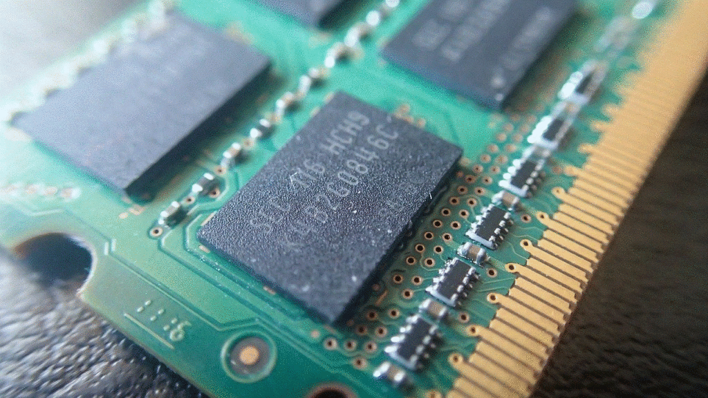
Moore’s Law results in more capacity in random access memory (RAM) chips.
Cheaper IC Components
Integrated circuits are not only increasing in computational capability as the technology is developed to increase transistor count. Transistor cost also decreases over time, as the manufacturing cost per transistor does not scale with the number of transistors. The higher the density of transistors, the lower the per transistor cost in a chip. This has allowed processor cost to remain relatively low even as performance improves.
Over time, the cost of IT equipment has declined significantly.
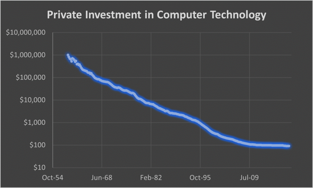
Data from US Bureau of Economic Analysis
Limitations of Moore’s Law
Despite decades of achieving Moore’s Law, there are several limitations that have resulted in skepticism regarded its’ continued viability. Forecasters have prophesied the end of Moore’s Law for well over a decade. In 2005, Gordon Moore himself predicted that Moore’s Law would continue to hold for only another decade or two.
Transistor Size Limitations
One of the main problems faced by the semiconductor industry is that transistors can’t be reduced endlessly. Transistors are devices that rely on the properties of the whole system, but when they are too small, the quantum effects of the atoms themselves start to play a larger role. Further, even if quantum effects can be reduced enough to produce workable transistors, there is still a size floor due to the atoms themselves. A silicon atom itself is around .2nm, so even at the limits of single atom transistor dimensions, we will soon approach a fundamental limit.
A related problem is that the cost of developing and producing smaller components may be so high that the world is not willing to pay for companies to keep up the pace.
Difficulty of Fabrication
As transistors decrease in size, it becomes increasingly difficult to fabricate them on the mass scales required by the industry. Individual labs may be able to develop transistors with atom-sized features, but advances in fabrication technology are necessary for large scale production. Currently we have not developed sufficient fabrication technology to facilitate large scale production of transistors with atomic scale features.
Moore’s Second Law
A lesser known ‘Law’, considered the economic consequence of Moore’s Law, is that the cost of a semiconductor fabrication facility increases in cost over time. The capital investment required to stay apace of Moore’s Law grows at an exponential rate, making it more difficult to acquire necessary financing. As of 2015, the cost of a fabrication facility was around $14 billion.
Less Perceived Improvement from Moore’s Law
Even as Moore’s Law has led to incredible gains, computer user experience depends as much on software as it does on hardware. Over time, software has experience what is termed software bloat. With each successive generation, software tends to become more complex and packed with more features. While these features may be useful, they also increase required resources and processing time. Despite superior hardware, software bloat results in a worse user experience. This is why computers don’t actually seem as fast as they ostensible should be, based on Moore’s Law.
Is Moore’s Law Slowing?
Technology Nodes and Transistor Size
In order to help track semiconductor developments, manufacturers began tying their products to what were called technology nodes.
These technology nodes were named after the size of a specific transistor feature. For instance, the 32 nm node, which began in 2010, featured transistors with corresponded with the average transistor gate length of less than 32 nanometers.
However, the 32 nm node was the last technology node for which this was the case. The 22nm node represented a switch to FinFETs, which allowed a higher transistor density despite larger feature sizes.
Even though transistor size is no longer the dominant factor, manufacturers have been able to closely track Moore’s Law by increasing transistor density via new transistor designs and chip architecture.
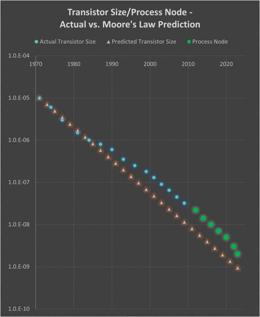
The plot on the right shows the trend of actual transistor size as well as the post-32nm node representations, vs. the actual transistor size predicted by Moore’s Law.
We can see that transistor size scaling has not matched the Moore’s Law since 1987, but has tracked it closely.
This plot also shows future nodes that are anticipated by semiconductor companies. The 5nm process is currently in production by both Samsung and TSMC. The 3nm process has been announced as the next die shrink node, expected to be in volume production by 2022. A 2nm process, the next die shrink node after 3nm, is expected to begin risk production around 2024.
As we can see, these new process nodes may extend the progress predicted by Moore’s Law at least until the mid-2020’s. In fact, if manufacturers achieve production by their own anticipated timelines, the 3nm and 2nm processes may represent an increased pace of development compared with the historical trend.
Transistor Density
According to data from Intel, developments over the last decade have actually increased the rate of transistor density improvement.
This is a clear indicator that the industry is closely adhering to Moore’s Law. If future technology nodes continue to deliver on the promises of manufacturers, Moore’s Law may continue to apply for the foreseeable future.
New Transistor Technologies: Nanowire/Nanoribbon Transistors
New transistors that are in development by manufacturers like Intel and Samsung hold significant potential for future improvements.
One example is the so-called nanowire or nanoribbon transistor. Nanoribbon transistors have a narrow, 3-D design and are expected to enable transistor density to be increased as much as 4x. According to Intel, production of nanoribbon transistors are expected within the next 5 years. Samsung has similar technologies in development that offer the promise of huge improvements to transistor density in integrated circuits.
Conclusion
While there are many competing factors at play, for the time being it appears that the semiconductor industry will continue to be able to adhere closely to Moore’s Law.
Manufacturers are maintaining a feverish pace to develop new technologies that promise to deliver the pace of improvement we have been used to over the last five decades.
Perhaps one of the most important limiting factors will be capital investment in fabrication plants. As the perceived benefit of development declines (despite technological progress), it may become increasingly difficult and therefore take longer to acquire necessary capital funding for new, large scale processes. This problem may be compounded by the increasing costs of fabrication facilities themselves.
Thus, capital investment may become more of a factor in any perceived decline of Moore’s Law. The technology may be sufficiently developed, but the capital required for large scale production could become a limiting factor in the near future.
