What is a Printed Circuit Board (PCB)?
A printed circuit board, or PCB, is a board made of an insulating material that contains conductive pathways etched onto its surface. Circuit components are mounted to the surface of the PCB, with the board taking the place of connecting wires and providing a helpful structure for the circuits.
Printed circuit boards are commonly made with fiberglass or a composite material. The conductive pathways are typically made of copper, and are used to connect different electronic components together in a circuit. PCBs can be single-layer, double-layer, or multi-layer, depending on the complexity of the circuit they are designed to support.
PCBs are used in a wide range of applications, from simple devices such as calculators and digital watches, to complex systems such as computers and smartphones. Virtually every modern electronic device today contains PCBs. The process of designing and manufacturing PCBs involves specialized software and equipment, and is an important part of the electronics industry.
In this article, we will do a deep dive on printed circuit boards. We’ll learn what PCBs are, how they are constructed, manufactured, designed, and even reverse-engineered.
- What is a Printed Circuit Board (PCB)?
What is a Printed Circuit Board (PCB)?
A printed circuit board (PCB) is a board made of insulating material with a thin layer of conductive material, typically copper, laminated onto its surface. The conductive layer is then etched to create a pattern of conductive pathways, or traces, which connect the different components on the board.
When a circuit on the PCB is powered, electricity flows through the conductive traces, providing power to the components and allowing them to perform their intended function. The traces are designed to provide the correct voltage and current levels to each component while minimizing interference and ensuring reliable operation.
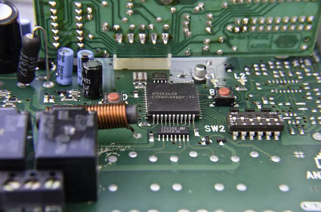
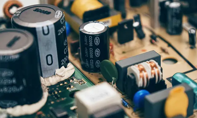
Components are mounted to the board in order to form useful circuits. The components mounted on a PCB can include resistors, capacitors, diodes, transistors, and integrated circuits, among others. Each component is connected to the PCB using a pad, which provides a metalized area for the component lead to be soldered to. The pads are connected to the traces using vias, which are small holes drilled through the board that are coated with conductive material.
The layout and routing of the traces on a PCB is an important factor in its performance and reliability. PCB designers need to consider factors such as the distance between components, the amount of current flowing through each trace, and the potential for interference from other components or external sources.
The Parts of a Printed Circuit Board
There are several important parts of a printed circuit board. Learning these will help you to understand how a printed circuit board actually works.
- Substrate: The base material on which the circuit is printed, usually made of a non-conductive material such as fiberglass.
- Surface: Where all the components are mounted onto (the surface of the board that you can see).
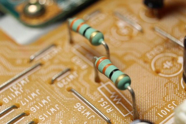
- Pad: A metalized area on the board used to connect a component lead to the circuit.
- Components: Circuit components are connected to the PCB by soldering through a hole (through-hole) or directly to a pad on the surface (surface-mount).
- Trace: A conductive pathway on the board that connects different components together. Traces look like lines, or pathways, on the surface that connect the components into useful circuits.
- Via: A small hole that connects different layers of the PCB together.
The Surface
The surface of a printed circuit board is where the components and conductive traces are located. The surface can be either single-sided or double-sided, depending on the design of the circuit.
On a single-sided PCB, components and conductive traces are located only on one side of the board, while the other side is usually left blank. Double-sided PCBs have components and traces on both sides of the board, connected by through-hole vias or surface-mounted vias.
The surface of a PCB can also be covered with a layer of solder mask. Solder mask is a protective coating that helps to prevent shorts and other types of damage to the board. Solder mask is usually green in color, but other colors can also be used.
In addition to solder mask, the surface of a PCB can also be covered with a layer of silkscreen, which is a layer of printing that provides labels, component identifications, and other information about the board. The silkscreen is usually white in color and is applied using a specialized printing process.
Overall, the surface of a PCB is an important component of its design and performance, as it determines the location of the components and the routing of the conductive traces. The surface can also be protected and labeled using various coatings and printing techniques to ensure the reliability and functionality of the board.
PCB Traces
A PCB trace is a thin copper line etched onto a printed circuit board (PCB) that serves as a conductive pathway between different components on the board. PCB traces are used to connect components, carry signals and power, and create electrical paths between different parts of a circuit.
The width, thickness, and spacing of a PCB trace can all affect its electrical properties, such as its resistance and capacitance. The size of the trace is typically determined by the amount of current that needs to flow through it, as larger currents require wider traces to avoid overheating and damage to the board.
PCB traces can be routed on the surface layer of the board or on inner layers, depending on the complexity of the circuit and the number of components that need to be connected. In multi-layer PCBs, vias are used to connect the traces on different layers.
PCB traces are an essential part of modern electronics, as they allow for precise and reliable connections between different components on a circuit board. PCB designers must carefully consider the layout and routing of traces to ensure that the circuit functions correctly and reliably.
PCB Vias
A via is a small hole drilled into a printed circuit board (PCB) that is used to create an electrical connection between different layers of the board. Vias can also be used to connect components on opposite sides of the board.
Vias typically consists of a hole that is drilled through the substrate material of the PCB and then coated with a thin layer of conductive material, such as copper. The copper plating on the inside of the hole creates a conductive pathway between the different layers of the PCB.
There are several types of vias that are commonly used in PCB design, including:
- Through-hole via: A simple via that goes all the way through the board from one side to the other.
- Blind via: A via that starts on the surface of the board and only goes part-way through the substrate, connecting one or more inner layers of the board.
- Buried via: A via that starts and ends within the substrate of the board, connecting two or more inner layers of the board without breaking through to the surface.
Vias are an important part of PCB design, as they allow for complex circuits to be created with multiple layers and connections. They are used in a wide range of applications, from simple electronic devices to complex computer systems.
PCB Pads
The pad is a metalized area on a printed circuit board used to provide a connection point for a component lead. In other words, components are soldered to the pads on the PCB.
Pads are typically circular or rectangular in shape, and are located at specific locations on the board according to the component placement.
The size and shape of the pad are designed to accommodate the lead of the component that will be soldered to it. Pads can be plated or unplated, depending on the application. Plated pads have a thin layer of conductive material, usually copper, applied to the surface of the pad, which helps to improve the electrical connection between the component and the PCB.
Pads can be connected to the conductive traces on a PCB using vias. The vias allow the connection to be made between the surface layers of the board and the inner layers where the traces are located.
Pads are an essential component of PCB design, as they provide a reliable and efficient way to connect components to the board. The design of the pads and their placement on the board are important factors that must be carefully considered to ensure that the PCB functions reliably.
Why Are PCBs Popular?
Printed circuit boards have become incredibly popular over the years due to their many advantages over other types of wiring and connection methods. One of the main reasons for their popularity is their cost-effectiveness. PCBs can be mass-produced using automated processes, which reduces the manufacturing cost and makes them a more affordable option for electronic manufacturers. Additionally, PCBs provide a high level of consistency and accuracy in their manufacturing process, ensuring that each board is identical in its layout and performance, which enhances reliability and reduces the risk of loose connections or other wiring problems.
PCBs are also highly space-efficient and can be designed to be very compact, which makes them ideal for use in miniaturized electronic devices. They allow for a high density of electronic components to be mounted on a single board, thereby reducing the need for additional wiring and space required for wiring.
Another advantage of PCBs is that they can provide better signal integrity than other wiring methods, such as wire-wrap or point-to-point wiring. By minimizing electromagnetic interference and signal loss, PCBs offer a more reliable and efficient way of transmitting electrical signals between components.
Finally, PCBs are easy to assemble, either by hand or more commonly using automated assembly machines, which reduces the time and labor required for manufacturing.
Types of PCBs
There are several types of printed circuit boards available, each with its own unique features and applications. Here are some of the most common types:
- Single-sided PCB: This is the most basic type of PCB, with components and conductive traces located only on one side of the board.
- Double-sided PCB: A double-sided PCB has components and conductive traces located on both sides of the board, connected by through-hole vias or surface-mounted vias.
- Multilayer PCB: The multilayer PCB has multiple layers of conductive traces and insulating material, allowing for more complex circuit designs. The layers are connected using vias.
- Rigid PCB: Rigid PCBs are made of a rigid material, such as fiberglass or epoxy. They are suitable for applications where the board will not be subjected to bending or flexing.
- Flexible PCB: A flexible PCB is made of a flexible material, such as polyimide, and is suitable for applications where the board will be subjected to bending or flexing.
- HDI PCB: High-density interconnect (HDI) PCBs are designed to have higher component density and smaller vias. This allows for more compact and efficient designs.
- Metal Core PCB: This type of PCB has a metal core to help dissipate heat from high-power components. The core is usually made of aluminum.
- Ceramic PCB: PCBs can also be made of ceramic material like alumina. Ceramic PCBs are often suitable for high-temperature applications.
The choice of PCB type depends on the specific requirements of the application, including the complexity of the circuit, the available space, and the desired performance characteristics.
How Are PCBs Manufactured?
Printed circuit boards (PCBs) are manufactured using a series of steps that involve a combination of design, fabrication, and assembly processes. Here’s a brief of the PCB manufacturing process:
- Design: The first step in PCB manufacturing is to create a design for the board using specialized software. The design specifies the placement of components, the routing of traces, and all of the other important details about the board.
- Fabrication: The fabrication process involves the creation of the physical board based on the design. This typically involves a combination of printing, etching, and drilling processes.
- Inner layer creation: If the PCB is a multi-layer board, the inner layers are created by laminating copper-clad sheets of fiberglass or other materials together, along with the copper layers sandwiched between the insulating layers.
- Drilling: Holes are drilled through the board to create the vias that connect the layers of the board.
- Plating: A layer of metal, usually copper, is applied to the board to create the conductive traces and pads. This is done using an electroplating process, which covers everything in a layer of copper.
- Etching: A chemical process is used to remove the excess copper and create the desired circuit pattern.
- Solder mask application: A layer of solder mask is applied to the board to protect the copper traces from damage and to help prevent shorts.
- Silkscreening: Ink is printed on the board to provide labeling and other information.
- Assembly: Once the board is manufactured, it can be populated with electronic components using various assembly processes, such as surface mount technology (SMT) or through-hole technology.
PCB manufacturing is a complex process that involves multiple steps and highly specialized equipment. The specific details of the process may vary depending on the design of the board and the requirements of the application.
The PCB Design Process
The PCB design process involves a series of steps to create a layout for a printed circuit board that meets the desired requirements and specifications. Here’s a general overview of the PCB design process:
- Defining the specifications: The first step in the PCB design process is to define the specifications of the board, including its size, shape, number of layers, and electrical requirements.
- Schematic capture: Once the specifications are defined, the next step is to create a schematic diagram of the circuit. This involves identifying the components needed for the circuit, as well as their interconnections.
- PCB layout design: After the schematic is created, the next step is to create the PCB layout. This involves placing the components on the board and routing the electrical connections between them using a specialized software tool.
- Design verification: Once the layout is completed, the design is verified to ensure that it meets the desired specifications and requirements. This may involve running simulations and performing design rule checks (DRCs) to ensure that the board can be manufactured and assembled correctly.
- Gerber file generation: After the design is verified, the Gerber files are generated. These files contain the data needed to manufacture the board, including the component placements, trace routing, drill holes, and other details.
- PCB fabrication: The Gerber files are sent to a manufacturer who produces the PCB according to the design specifications.
- Assembly: Once the PCB is manufactured, the final step is to assemble the components onto the board. This involves soldering the components onto the PCB using either surface-mount technology (SMT) or through-hole technology.
As you can tell, the PCB design process involves multiple steps and requires a combination of technical knowledge, specialized software tools, and attention to detail to ensure that the board meets the desired specifications and requirements.
How Much Does it Cost to Make a PCB?
The cost of a custom printed circuit board (PCB) can vary widely depending on a variety of factors, including the size, complexity, number of layers, and the quantity needed. Other factors that can affect the cost include the type of components used, the type of finish applied to the board, and the turnaround time required.
That said, you can get PCBs made for as low as just a few dollars on several of the major PCB manufacturer websites.
Through-Hole or Surface Mount?
Through-hole and surface mount are two common methods for mounting electronic components on a printed circuit board. The main differences between through-hole and surface mount PCBs are:
- Mounting method: Through-hole components have wire leads that are inserted into holes drilled in the PCB, and then soldered onto pads on the opposite side of the board. Surface mount components are mounted directly on the surface of the PCB and are soldered onto pads or lands on the same side of the board.
- Component size: Through-hole components are typically larger than surface mount components, due to the need for wire leads. Surface mount components can be much smaller and have a higher component density on the PCB.
- Assembly process: Through-hole components require manual insertion and soldering, while surface mount components can be mounted using automated pick-and-place machines and reflow soldering.
- PCB design: Through-hole components require larger and more spaced out pads and traces on the PCB to accommodate the wire leads, while surface mount components require smaller and closer spaced pads and traces to accommodate their small size.
In general, surface mount technology (SMT) has become more popular due to its ability to produce smaller and more complex PCBs with higher component densities, making them more suitable for modern electronics. However, through-hole components are still used for certain applications that require higher mechanical strength, higher current carrying capacity, or for components that need to be replaced easily.
Reverse Engineering a PCB
Reverse engineering a PCB involves taking an existing board and creating a detailed schematic and layout from it. Here are the general steps to reverse engineer a PCB:
- Document the board: Take high-resolution photos of the PCB from multiple angles, and document the component placements, trace routing, and any other relevant information about the board.
- Identify the components: Identify the type and value of each component on the board, and document this information in a spreadsheet or other format.
- Trace the circuit: Using a multimeter or other testing equipment, trace the electrical connections between the components on the board. Document this information on the schematic diagram.
- Create the schematic: Using the documented information from steps 1-3, create a detailed schematic diagram of the board.
- Create the layout: Using the schematic, create a layout of the board. This can be done using specialized software tools or by creating a physical template of the board and tracing the connections.
- Verify the design: Once the layout is completed, verify the design to ensure that it matches the original board. This can be done by comparing the new layout to the original board or by testing the new board to ensure that it functions correctly.
It’s important to note that reverse engineering a PCB can be a complex and time-consuming process, and it may be difficult to create an exact replica of the original. Additionally, reverse engineering may not be legal in all situations, so it’s important to verify the legality of reverse engineering any specific piece of technology before attempting this process.
In What Applications Are PCBs Not Used?
Printed circuit boards are not used in applications where the electrical components require a high degree of mobility, flexibility or in some applications where the design is highly customized. For example, in wearable technology, where the device is worn directly on the body, a flexible PCB or flexible printed electronics may be used instead of a rigid PCB to provide flexibility and comfort.
Similarly, in some cases, specialized or one-of-a-kind electronic devices may require custom wiring, rather than using a standard PCB. This may be the case in situations where the device needs to be highly adaptable, or if the device needs to be designed to fit a specific space or shape.
Another example where PCBs may not be used is in some types of high-frequency applications, where the circuitry is highly sensitive to electromagnetic interference (EMI) or signal loss. In these applications, alternative wiring methods such as wire-wrap or point-to-point wiring may be used instead to minimize EMI and signal loss.
While PCBs are versatile and widely used in various industries, they may not be suitable for every application. The decision to use a PCB or an alternative wiring method will depend on the specific requirements of the application, including factors such as cost, reliability, space constraints, and frequency requirements.